
- Joined
- Nov 4, 2019
- Messages
- 24
- Likes
- 169
This guide is a mirror of the guide posted on my GitHub repository.
The following guide will cover every step of the chip trimming process as best as possible, while also going over the various caveats, complications, and best practices. It will also go over the best workflow and order of operations.
While any chip with a leadframe can be trimmed in roughly the same manner/using the same steps, this guide is specifically geared towards NES chips in particular which are DIP40.
DISCLAIMER
Trimming the chips required for TinyTendo is a risky, delicate, and tedious process, and may result in irreparable damage to your hardware (chips), and due to the use of power tools, injury could occur if not done properly.
I am not responsible for any damage at all done to you or your hardware, follow this guide at your own risk.
REQUIREMENTS
* Eye and respiratory protection
* Rotary Tool (Dremel)
* Flex wand for rotary tool (Optional, but highly recommended)
* Diamond rotary tool cutting wheel
* Rotary tool sanding drum bit, with fine grit sandpaper (600 grit at least is preferable)
* Sandpaper (320 at least is recommended)
* Caliper (Preferably digital)
* Sharp marking tool (An exacto/craft knife was used in this guide)
* Straight edge (can be a ruler)
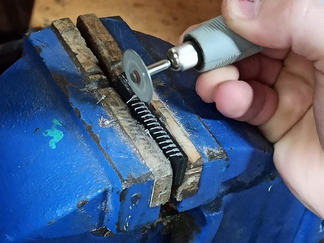
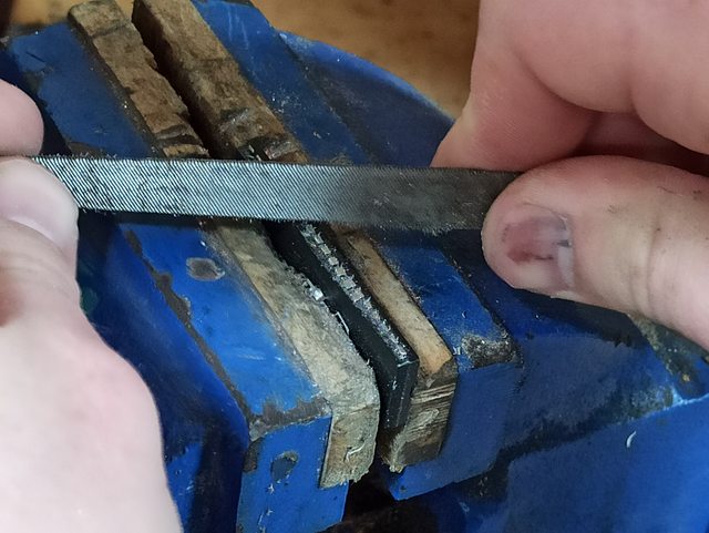
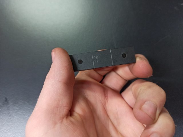
STEP 1 Remove leads
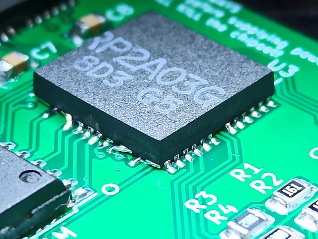
In order to trim the chips, the first step is to remove the leads, this is done by first cutting the majority of them off with a rotary tool cutting wheel, and then filing the remainder off until they are flush with the edge of the package.
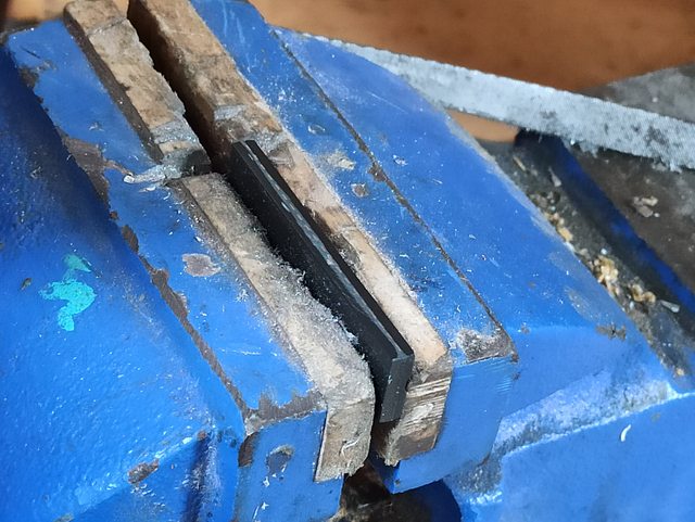
When finished with this step, the chip should look like this:
Optionally, to reduce the time required to complete the next step you can cut 15mm off of each end of the chip. (This will leave you with less to hold into when cutting, though.)
This will result in something looking like this:
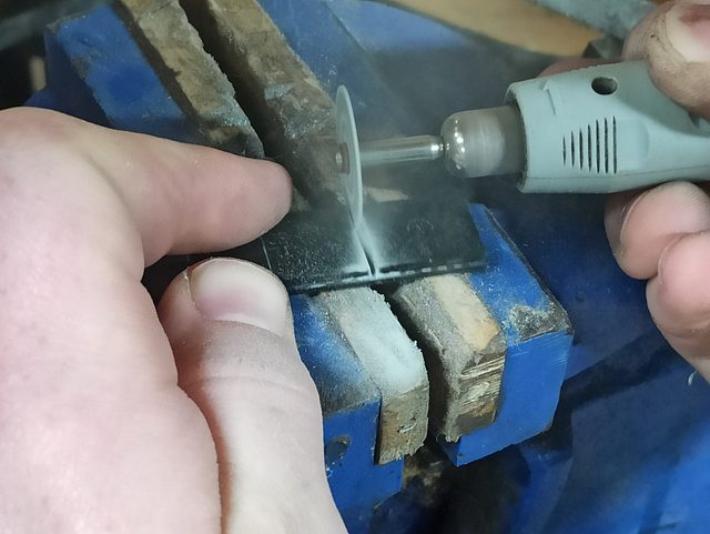
STEP 2 Grind Package
The next step is the the most time consuming part, and requires a great deal of care to do properly.
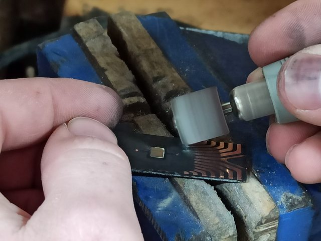
The package of the chip must be ground away from the bottom to expose the leadframe and die. This is done using a rotary tool sanding drum.
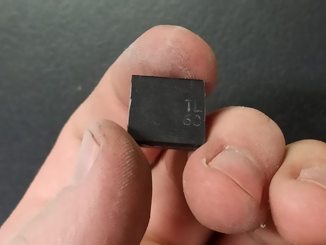
While grinding away the package, the first internal feature you will encounter is the die pad, this is what the silicon die is attached to within the chip. When you reach this pad, it is recommended to focus your attention to sanding the surrounding areas to expose the leadframe, and remove the die pad after the rest is exposed. This helps prevent damage to the die.
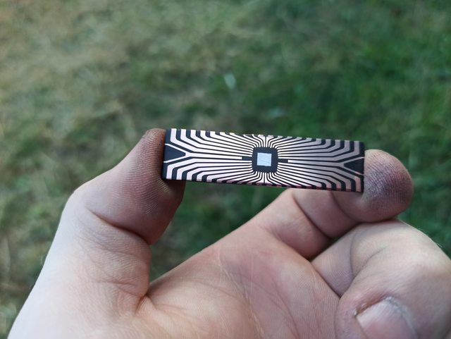
The die pad will look like this:
(The die pad is removed in the following photo, but should not be removed yet for you, it was removed due to the way the chip was prepared for the guide photos)
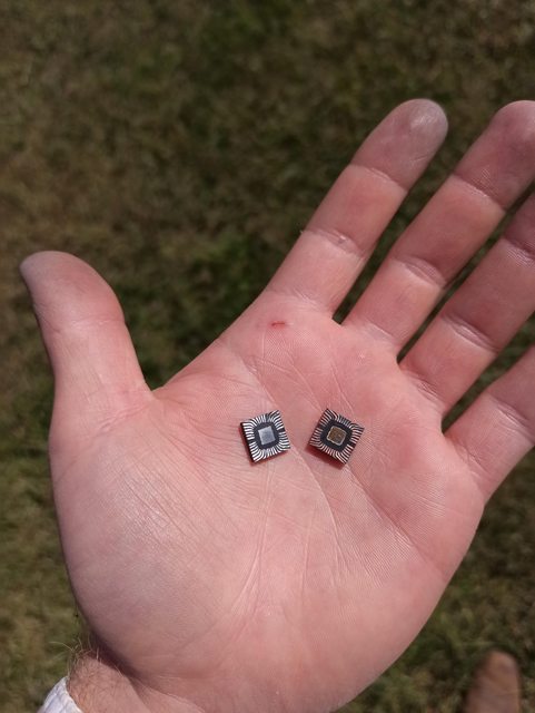
The result should look like this:
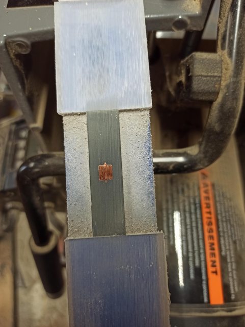
STEP 3A Mark Cut Line
The 3rd and final step is to cut the now ground down chip down to size, this is perhaps the easiest step to mess up and the most complex so it needs quite a bit of explanation.
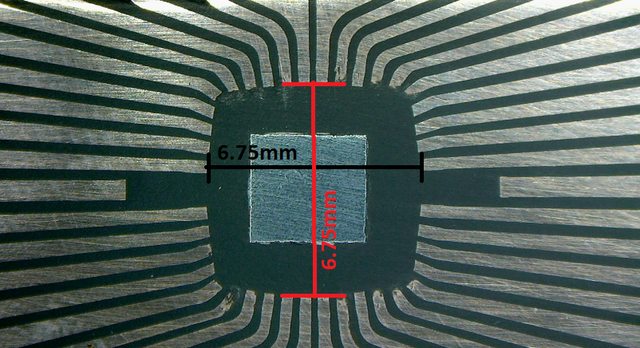
Firstly there are complications in measuring/marking the cut line for trimming the chip.
The first complication is that due to manufacturing inaccuracies the external dimensions of the chip can vary by as much as +/- 0.3mm in any or all of the 3 dimensions, this means you cannot mark the cut line from the external dimensions.
Additionally, the silicon die can also vary in placement within the chip by some amount in any of the 3 dimensions, this means you cannot mark the cut line by referencing the die.
The only method of measuring/marking the cut line is by referencing the leadframe ends, or more specifically the opening in the leadframe.
This is why we ground the chip before cutting, as we cannot cut the chip without being able to see the leadframe.
The dimensions of the leadframe opening on your chip may be different than the chip shown, but the measurements for my chip are shown below:
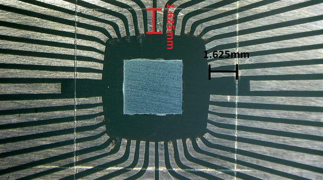
Next we need to cut the chip down to size, this is the point of no return so to speak.
If this is not done correctly the chip will be dead. If the chip is too large, it will not fit or may not line up with the motherboard footprint, too small and you could break the wirebonds and kill the chip.
IMPORTANT
The chip should be exactly 10x10mm, and ideally no bigger and no smaller, however up to 10.2mm should line up.
You must follow the diagrams shown previously to determine your cut line, but substitute the measurements with your own that match the chip you have.
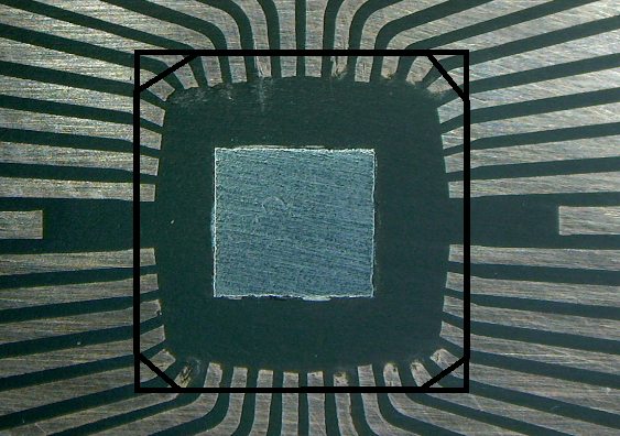
The following image shows the "keep out" area, above all else you must not cut cut/sand to this point, as you WILL sever the wirebonds and KILL the chip:
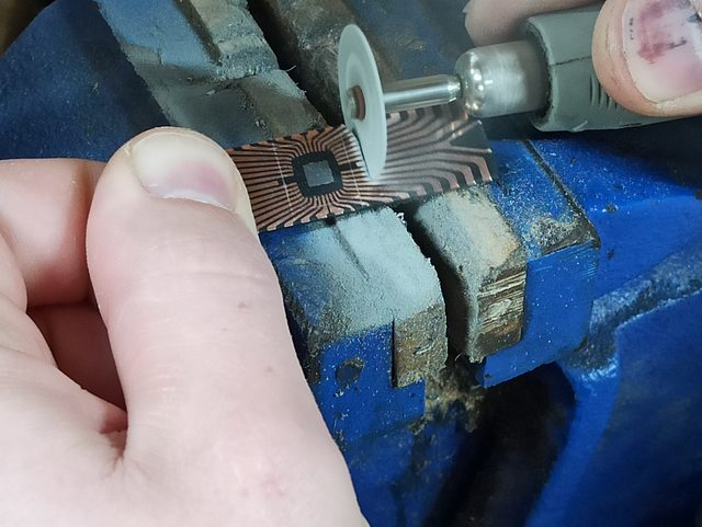
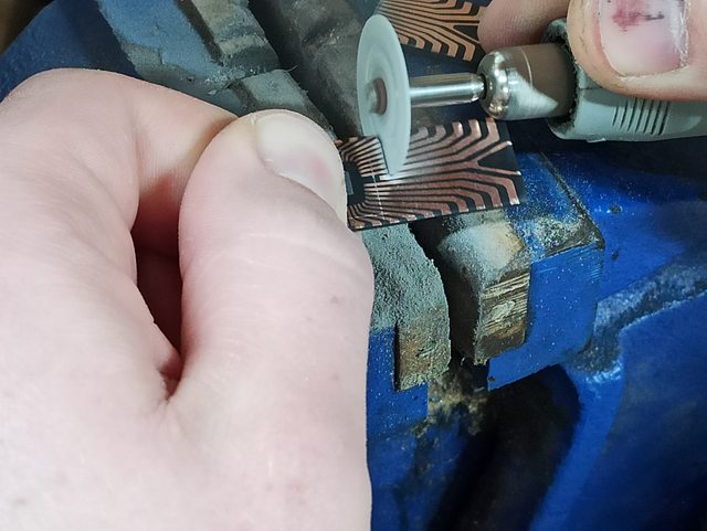
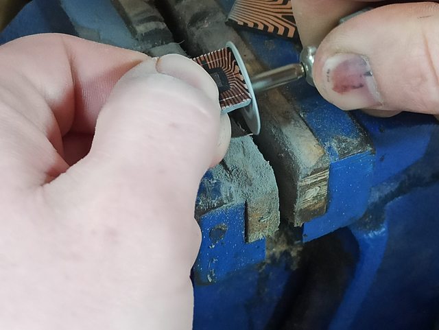
STEP 3B Cut Chip
To cut the chip, we will use a cutting wheel to remove excess material from the chip.
It is highly recommended that you cut away from the line, and work your way in with sandpaper after, as it will help prevent cutting off too much material.
The ideal workflow is to cut one of the ends first, repeat for the other end, then to use the face of the cutting wheel to grind inwards towards the line for the edges. (You may also use this technique to grind close inwards close to the other lines to reduce hand sanding time later, but you must be careful)
You must also be mindful of the direction the cutting wheel is spinning at all times during this process, if upward force is applied to the leadframe leads, they could peel out and kill the chip. When cutting, the direction of the wheel rotation must always run either parallel to the leadframe, or apply downward force to it, this is incredibly important to keep track of.
Cut end:
Repeat for other side:
Grind edges:
Once this is complete, we are almost done.
All that is left to do is to manually hand sand the edges of the now cut chip until it is 10x10mm.
Make sure to frequently measure with calipers in order to make sure you have sanded enough, and haven't sanded too much.
It is also recommended to visually check whether the chip lines up with the motherboard footprint on all sides frequently.
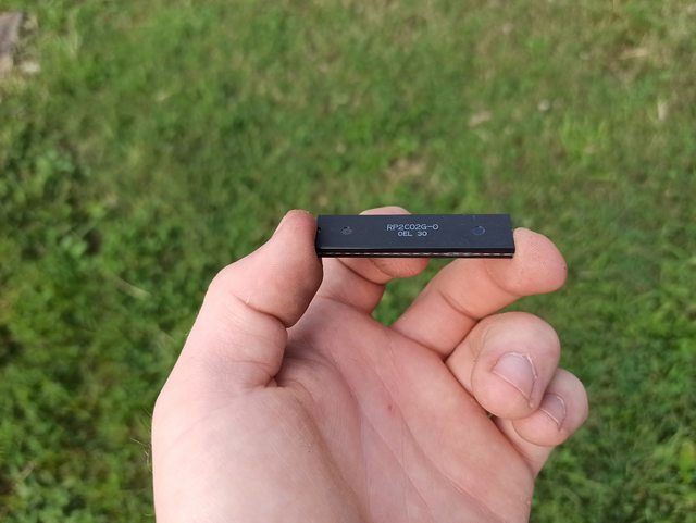
When all is said and done, the final chips should look like this:
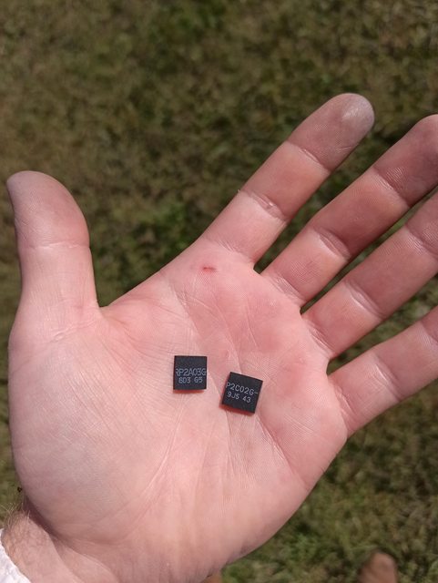
The chip(s) are now ready to be soldered onto the TinyTendo motherboard.
The process to do so is identical to that of soldering a standard QFN package, as such I don't feel it needs additional explanation.
Have fun playing all the LJN NES titles you could ever dream of while on the go!
The following guide will cover every step of the chip trimming process as best as possible, while also going over the various caveats, complications, and best practices. It will also go over the best workflow and order of operations.
While any chip with a leadframe can be trimmed in roughly the same manner/using the same steps, this guide is specifically geared towards NES chips in particular which are DIP40.
DISCLAIMER
Trimming the chips required for TinyTendo is a risky, delicate, and tedious process, and may result in irreparable damage to your hardware (chips), and due to the use of power tools, injury could occur if not done properly.
I am not responsible for any damage at all done to you or your hardware, follow this guide at your own risk.
REQUIREMENTS
* Eye and respiratory protection
* Rotary Tool (Dremel)
* Flex wand for rotary tool (Optional, but highly recommended)
* Diamond rotary tool cutting wheel
* Rotary tool sanding drum bit, with fine grit sandpaper (600 grit at least is preferable)
* Sandpaper (320 at least is recommended)
* Caliper (Preferably digital)
* Sharp marking tool (An exacto/craft knife was used in this guide)
* Straight edge (can be a ruler)
STEP 1 Remove leads
In order to trim the chips, the first step is to remove the leads, this is done by first cutting the majority of them off with a rotary tool cutting wheel, and then filing the remainder off until they are flush with the edge of the package.
When finished with this step, the chip should look like this:
Optionally, to reduce the time required to complete the next step you can cut 15mm off of each end of the chip. (This will leave you with less to hold into when cutting, though.)
This will result in something looking like this:
STEP 2 Grind Package
The next step is the the most time consuming part, and requires a great deal of care to do properly.
The package of the chip must be ground away from the bottom to expose the leadframe and die. This is done using a rotary tool sanding drum.
While grinding away the package, the first internal feature you will encounter is the die pad, this is what the silicon die is attached to within the chip. When you reach this pad, it is recommended to focus your attention to sanding the surrounding areas to expose the leadframe, and remove the die pad after the rest is exposed. This helps prevent damage to the die.
The die pad will look like this:
(The die pad is removed in the following photo, but should not be removed yet for you, it was removed due to the way the chip was prepared for the guide photos)
The result should look like this:
STEP 3A Mark Cut Line
The 3rd and final step is to cut the now ground down chip down to size, this is perhaps the easiest step to mess up and the most complex so it needs quite a bit of explanation.
Firstly there are complications in measuring/marking the cut line for trimming the chip.
The first complication is that due to manufacturing inaccuracies the external dimensions of the chip can vary by as much as +/- 0.3mm in any or all of the 3 dimensions, this means you cannot mark the cut line from the external dimensions.
Additionally, the silicon die can also vary in placement within the chip by some amount in any of the 3 dimensions, this means you cannot mark the cut line by referencing the die.
The only method of measuring/marking the cut line is by referencing the leadframe ends, or more specifically the opening in the leadframe.
This is why we ground the chip before cutting, as we cannot cut the chip without being able to see the leadframe.
The dimensions of the leadframe opening on your chip may be different than the chip shown, but the measurements for my chip are shown below:
Next we need to cut the chip down to size, this is the point of no return so to speak.
If this is not done correctly the chip will be dead. If the chip is too large, it will not fit or may not line up with the motherboard footprint, too small and you could break the wirebonds and kill the chip.
IMPORTANT
The chip should be exactly 10x10mm, and ideally no bigger and no smaller, however up to 10.2mm should line up.
You must follow the diagrams shown previously to determine your cut line, but substitute the measurements with your own that match the chip you have.
The following image shows the "keep out" area, above all else you must not cut cut/sand to this point, as you WILL sever the wirebonds and KILL the chip:
STEP 3B Cut Chip
To cut the chip, we will use a cutting wheel to remove excess material from the chip.
It is highly recommended that you cut away from the line, and work your way in with sandpaper after, as it will help prevent cutting off too much material.
The ideal workflow is to cut one of the ends first, repeat for the other end, then to use the face of the cutting wheel to grind inwards towards the line for the edges. (You may also use this technique to grind close inwards close to the other lines to reduce hand sanding time later, but you must be careful)
You must also be mindful of the direction the cutting wheel is spinning at all times during this process, if upward force is applied to the leadframe leads, they could peel out and kill the chip. When cutting, the direction of the wheel rotation must always run either parallel to the leadframe, or apply downward force to it, this is incredibly important to keep track of.
Cut end:
Repeat for other side:
Grind edges:
Once this is complete, we are almost done.
All that is left to do is to manually hand sand the edges of the now cut chip until it is 10x10mm.
Make sure to frequently measure with calipers in order to make sure you have sanded enough, and haven't sanded too much.
It is also recommended to visually check whether the chip lines up with the motherboard footprint on all sides frequently.
When all is said and done, the final chips should look like this:
The chip(s) are now ready to be soldered onto the TinyTendo motherboard.
The process to do so is identical to that of soldering a standard QFN package, as such I don't feel it needs additional explanation.
Have fun playing all the LJN NES titles you could ever dream of while on the go!
Last edited:
