
Worklog Some PS2 Project
- Thread starter Tschicki
- Start date
- Joined
- Dec 2, 2022
- Messages
- 4
- Likes
- 12
great project, now let's talk about the custom rom! 
")
Tschicki
.
Update time!
MAX17320 fuel gauge & protector:
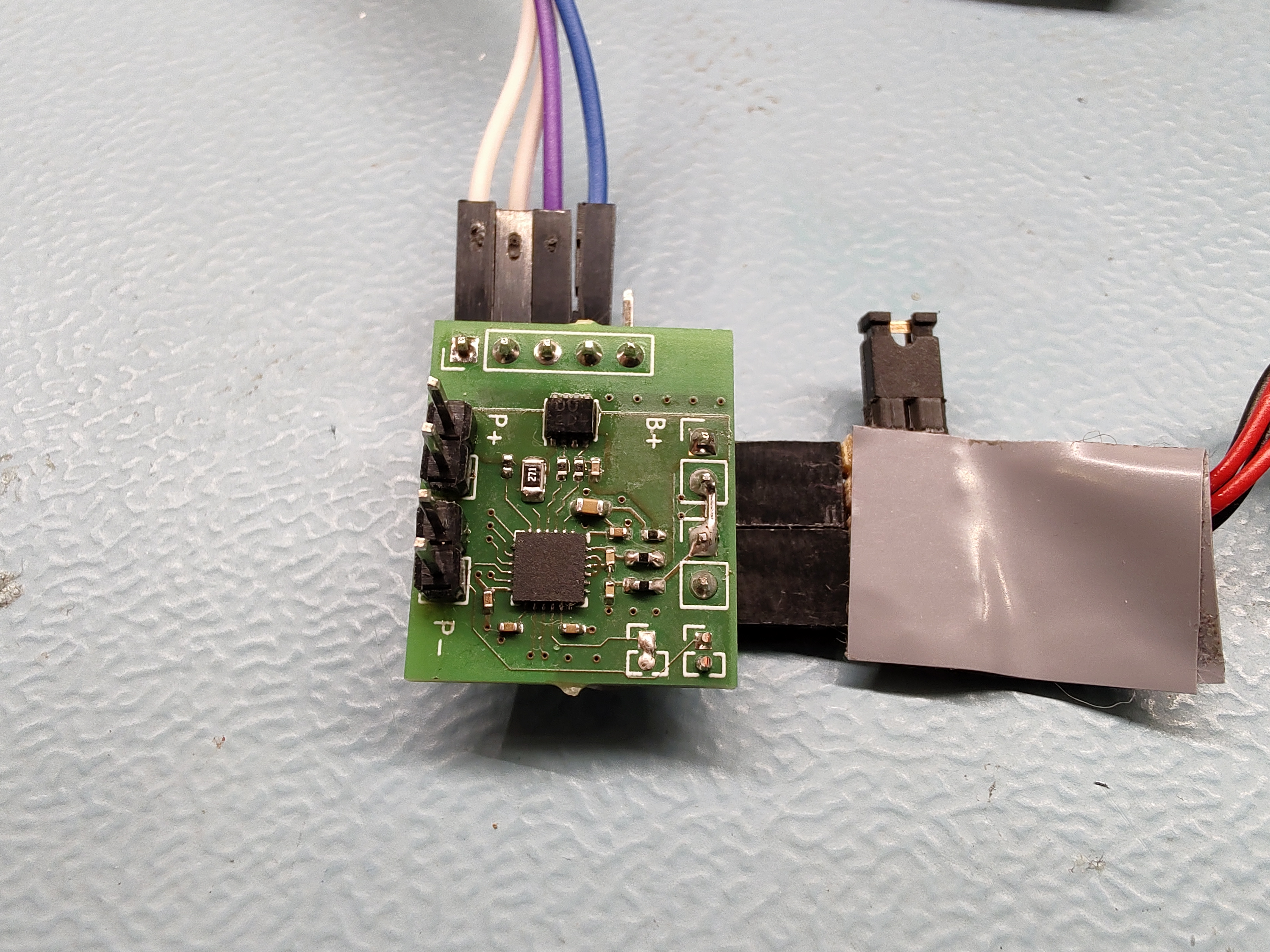
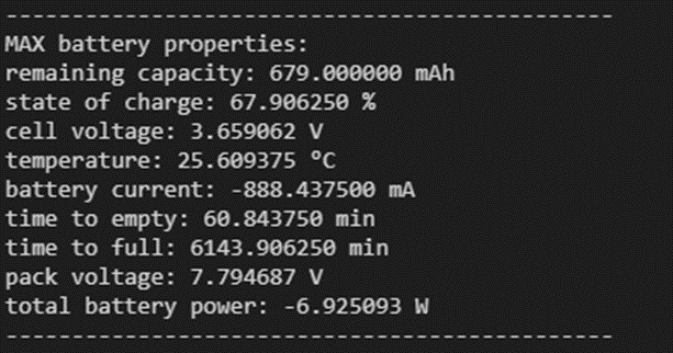
I received the PCB I designed around the MAX17320 and got one populated. The basic driver for it is up and running, it’s essential function right now is to get the battery properties: SOC, remaining capacity, cell and pack voltage, battery temperature, current, time to empty, time to full, and total system power draw.
On top of that it gets the status and fault registers of the chip. There is also a function to program the NVM with the exported configuration from the MAX17320 development software. Right now, I’m only displaying the data I read in the debug terminal, but the plan is to use the alert interrupts of the MAX, BQ and STUSB to handle charging/discharging faults.
I will think about which bits make sense to determine fault states and how I should process the analog readings in the firmware. This also includes handling charge termination, battery cutoff, and error recovery. Planning that takes a lot of time and effort, as I’m not a very experienced programmer, so I’m not done with that anytime soon.
SysCon:
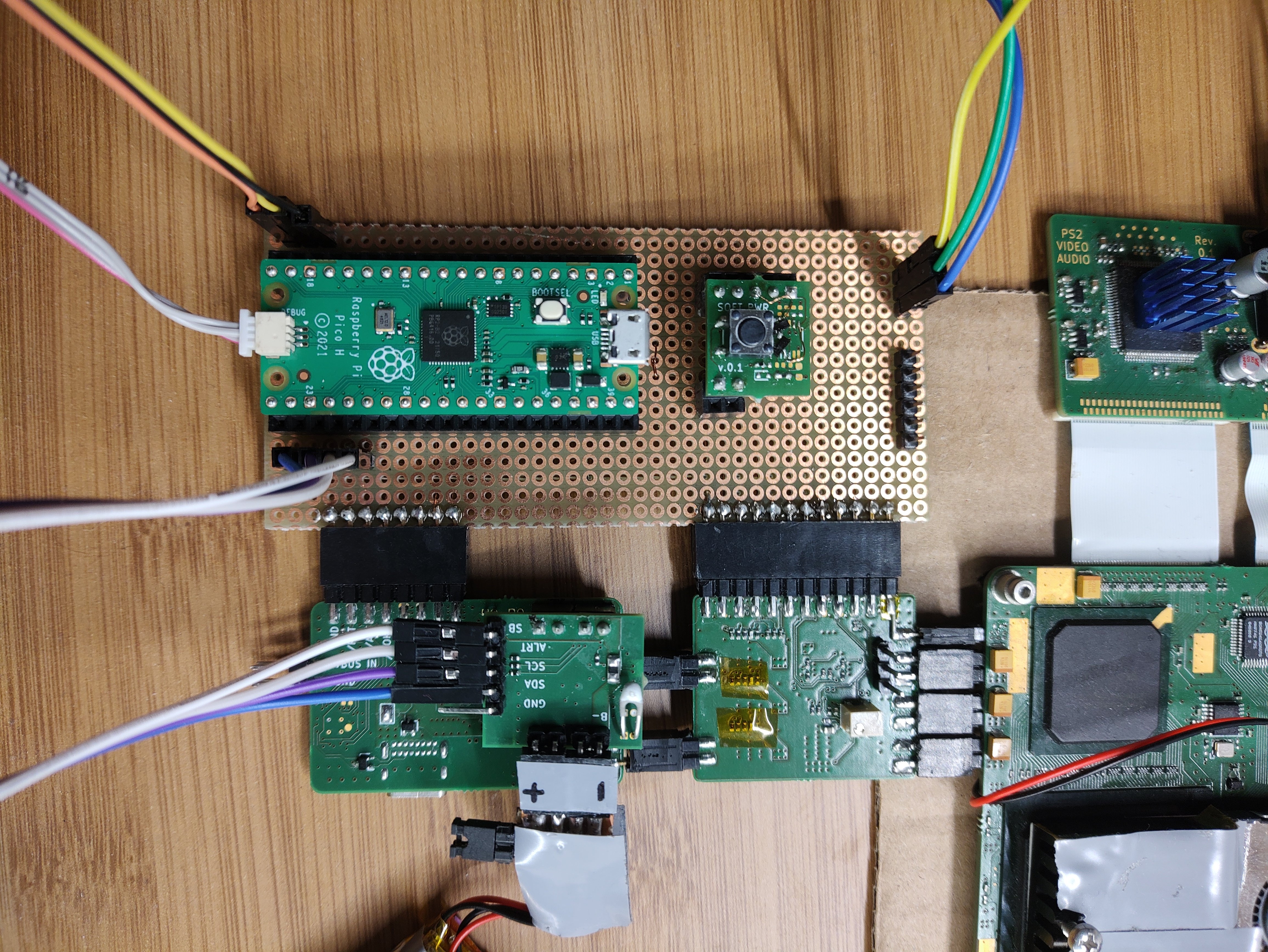
I finally decided for a microcontroller to use in the SysCon: the RP2040. Looking at the price, popularity and availability, it’s hard to find arguments against using it.
There is only one major drawback though, which is the development toolchain. In the last 3 weeks I was fighting with CMake, gcc, Eclipse, VSC and the pico SDK and it was not a great experience. Coming from the CubeIDE, my natural first step was to install Eclipse according to the “getting started” guide. I spent 2 weeks on that and it couldn’t even compile the example projects at the end.
Thankfully, @StonedEdge provided me with a link to a nice package for developing on the pico. It provides what the Raspberry Pi Foundation apparently cannot do: a development tool that pretty much works out of the box.
Nevertheless, I made a copy of the SysCon project and started porting the code. Thankfully only one file contained STM32 HAL functions (on purpose), so changing it was very straight forward. It took 2 evenings to port the project and now it’s finally working!
A pleasant surprise is that the pico debugger seems much more stable than the STLink. I can now plug and unplug chargers while debugging, even resetting the uC works while debugging. It makes testing and troubleshooting much easier!
There are some workarounds in the code currently, mainly involving the open drain outputs (or the lack of real OD outputs on the RP2040). The I2C write function is also quite quirky right now, because the pico SDK expects the register address to be in byte 0 of the RW buffer (on the STM32 it was handled separately). Now I have to move all bytes up by 1 in the RW array to make space for the register address, to avoid changing all my drivers.
The fact that all I2C and SPI functions of the pico SDK are blocking might create headaches in the future though. Overall, it works well and I will continue using it.
Gamepad:
Not much happened here, yesterday I started looking into the DS2 communication protocol and writing down commands and states. In the next weeks I will try to get some code working.
Customized BIOS:
I still can’t believe we got this one working! I was contacted 2 weeks ago by @Epaminondas, who is working on a modified BIOS to get rid of modchips and FMCB.
Hats off to you and thanks for sharing, your work is simply incredible!
He had the idea to patch the BIOS with the “PS2 Basic Bootloader, PS2BBL” to boot any application at startup, without requiring FMCB or a modchip. Apparently, there is some unused memory in the BIOS, so this could be done without breaking any functionality. It’s not enough to include OPL in the BIOS, but more than enough for PS2BBL.
It took us 2 troubleshooting sessions, but we got it working in the end! Unbelievable!
PS2BBL is the first thing to boot and it is searching for a config file on MC0/MC1/USB to get the paths for launching applications.
Epaminondas is developing a script to patch the BIOS automatically (and even change the BIOS region), I hope you will share it one day! From what I heard, he was able to include the config file in the bios too with the latest mod, so only OPL is required!
The drawback of this solution is that you still need OPL on either a USB stick or memory card. It is also required to put the config file on one of the attached storage devices. Another drawback of this exact BIOS mod in general is that the PS2 will most likely lose the ability to play disc games. Let me explain:
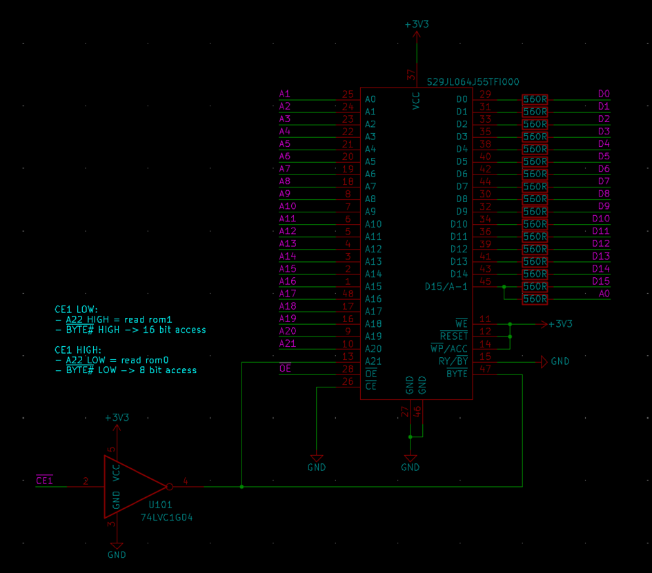
During our debugging we discovered that the BIOS chip is actually 64M. It includes the BIOS (rom0) in the lower 32M and the DVD ROM (rom1) in the upper 32M. By exchanging the chip with a 32M NOR flash, I accidentally removed the DVD ROM entirely without noticing (which is good, that’s why we know that we don’t need it…). After discovering that, we had the idea to recover the DVD ROM and to use it to store OPL/ULE.
For that I had to do some reverse engineering again. We knew that CE1 should read the DVD ROM and CE2 should read the BIOS, as seen in the 70k service manual. We also knew that the PS2 reads the BIOS in 8-bit mode and the DVD ROM in 16-bit mode. We were suspecting that the BIOS chip has some sort of CE decoding that required some further tests to find out which decoding is needed to successfully drive a NOR flash. The biggest question mark was the byte# and the A22 pin, as the CE of the chip can be tied to GND (by using the 560R resistors on the data lines, as proposed by @mixa232323).
The byte# and A22 pin needs to be LOW for reading the BIOS and HIGH for reading the DVD ROM.
The candidates for driving the byte# pin were CE1, CE2, pin 12, pin13 and A22 of the original chip. I ran a couple of tests while sniffing these pins with the logic analyzer, mainly to find out the states of the pins under various conditions. Also playing with the byte# and A22 to see where the boot would get stuck and where the console would crash. I finally found a functional connection by sending the inverted CE1 to byte# and A22. You may ask yourself why I’m not just using the uninverted CE2, but it doesn’t work. It seems like the console is trying to access the BIOS, even when both CE1 and CE2 are HIGH, so in that case both byte# and A22 must be LOW. They must be HIGH when CE1 is LOW and they must be LOW when CE2 is LOW.
D15 was a bit tricky, as it is used as A-1 or D15 by the NOR flash, depending on the byte# pin state. The original ROM has a dedicated pin for A-1 and doesn’t share it with D15. Here is the working diagram:
I didn’t test disc games, as I don’t have a slim with working disk drive, but PS2Ident seems to detect the DVD ROM. To test it I dumped a stock 79k rom0 and rom1, merged them, flashed them and dumped them again using PS2Ident. Both files match.
The sad reality is that (currently) it’s not possible to launch applications stored on rom1. Epaminondas has the theory that it features some kind of encryption and/or partitioning, so we’re stuck with rom0 for now. So that mod is kind of useless, unless you really want to play discs.
For the 32M mod (removing the rom1) we found later during testing that by inverting CE1 you could also successfully drive the CE of the NOR flash to get rid of the resistors. Previously I did it using the inverted XHCS of the DSP, but using CE1 is possible too and more elegent.
Huge thanks at this point to @Epaminondas for making this work! It takes a lot of skill and knowledge about the PS2 hardware to do such modifications to the BIOS. I’m really excited to see what you come up with when you receive your flash chips and I hope you will share your progress!
That's it!
MAX17320 fuel gauge & protector:
I received the PCB I designed around the MAX17320 and got one populated. The basic driver for it is up and running, it’s essential function right now is to get the battery properties: SOC, remaining capacity, cell and pack voltage, battery temperature, current, time to empty, time to full, and total system power draw.
On top of that it gets the status and fault registers of the chip. There is also a function to program the NVM with the exported configuration from the MAX17320 development software. Right now, I’m only displaying the data I read in the debug terminal, but the plan is to use the alert interrupts of the MAX, BQ and STUSB to handle charging/discharging faults.
I will think about which bits make sense to determine fault states and how I should process the analog readings in the firmware. This also includes handling charge termination, battery cutoff, and error recovery. Planning that takes a lot of time and effort, as I’m not a very experienced programmer, so I’m not done with that anytime soon.
SysCon:
I finally decided for a microcontroller to use in the SysCon: the RP2040. Looking at the price, popularity and availability, it’s hard to find arguments against using it.
There is only one major drawback though, which is the development toolchain. In the last 3 weeks I was fighting with CMake, gcc, Eclipse, VSC and the pico SDK and it was not a great experience. Coming from the CubeIDE, my natural first step was to install Eclipse according to the “getting started” guide. I spent 2 weeks on that and it couldn’t even compile the example projects at the end.
Thankfully, @StonedEdge provided me with a link to a nice package for developing on the pico. It provides what the Raspberry Pi Foundation apparently cannot do: a development tool that pretty much works out of the box.
Nevertheless, I made a copy of the SysCon project and started porting the code. Thankfully only one file contained STM32 HAL functions (on purpose), so changing it was very straight forward. It took 2 evenings to port the project and now it’s finally working!
A pleasant surprise is that the pico debugger seems much more stable than the STLink. I can now plug and unplug chargers while debugging, even resetting the uC works while debugging. It makes testing and troubleshooting much easier!
There are some workarounds in the code currently, mainly involving the open drain outputs (or the lack of real OD outputs on the RP2040). The I2C write function is also quite quirky right now, because the pico SDK expects the register address to be in byte 0 of the RW buffer (on the STM32 it was handled separately). Now I have to move all bytes up by 1 in the RW array to make space for the register address, to avoid changing all my drivers.
The fact that all I2C and SPI functions of the pico SDK are blocking might create headaches in the future though. Overall, it works well and I will continue using it.
Gamepad:
Not much happened here, yesterday I started looking into the DS2 communication protocol and writing down commands and states. In the next weeks I will try to get some code working.
Customized BIOS:
I still can’t believe we got this one working! I was contacted 2 weeks ago by @Epaminondas, who is working on a modified BIOS to get rid of modchips and FMCB.
Hats off to you and thanks for sharing, your work is simply incredible!
He had the idea to patch the BIOS with the “PS2 Basic Bootloader, PS2BBL” to boot any application at startup, without requiring FMCB or a modchip. Apparently, there is some unused memory in the BIOS, so this could be done without breaking any functionality. It’s not enough to include OPL in the BIOS, but more than enough for PS2BBL.
It took us 2 troubleshooting sessions, but we got it working in the end! Unbelievable!
PS2BBL is the first thing to boot and it is searching for a config file on MC0/MC1/USB to get the paths for launching applications.
- Keep in mind, PS2BBL is installed on the bios chip and not loading from USB / MC
Epaminondas is developing a script to patch the BIOS automatically (and even change the BIOS region), I hope you will share it one day! From what I heard, he was able to include the config file in the bios too with the latest mod, so only OPL is required!
The drawback of this solution is that you still need OPL on either a USB stick or memory card. It is also required to put the config file on one of the attached storage devices. Another drawback of this exact BIOS mod in general is that the PS2 will most likely lose the ability to play disc games. Let me explain:
During our debugging we discovered that the BIOS chip is actually 64M. It includes the BIOS (rom0) in the lower 32M and the DVD ROM (rom1) in the upper 32M. By exchanging the chip with a 32M NOR flash, I accidentally removed the DVD ROM entirely without noticing (which is good, that’s why we know that we don’t need it…). After discovering that, we had the idea to recover the DVD ROM and to use it to store OPL/ULE.
For that I had to do some reverse engineering again. We knew that CE1 should read the DVD ROM and CE2 should read the BIOS, as seen in the 70k service manual. We also knew that the PS2 reads the BIOS in 8-bit mode and the DVD ROM in 16-bit mode. We were suspecting that the BIOS chip has some sort of CE decoding that required some further tests to find out which decoding is needed to successfully drive a NOR flash. The biggest question mark was the byte# and the A22 pin, as the CE of the chip can be tied to GND (by using the 560R resistors on the data lines, as proposed by @mixa232323).
The byte# and A22 pin needs to be LOW for reading the BIOS and HIGH for reading the DVD ROM.
The candidates for driving the byte# pin were CE1, CE2, pin 12, pin13 and A22 of the original chip. I ran a couple of tests while sniffing these pins with the logic analyzer, mainly to find out the states of the pins under various conditions. Also playing with the byte# and A22 to see where the boot would get stuck and where the console would crash. I finally found a functional connection by sending the inverted CE1 to byte# and A22. You may ask yourself why I’m not just using the uninverted CE2, but it doesn’t work. It seems like the console is trying to access the BIOS, even when both CE1 and CE2 are HIGH, so in that case both byte# and A22 must be LOW. They must be HIGH when CE1 is LOW and they must be LOW when CE2 is LOW.
D15 was a bit tricky, as it is used as A-1 or D15 by the NOR flash, depending on the byte# pin state. The original ROM has a dedicated pin for A-1 and doesn’t share it with D15. Here is the working diagram:
I didn’t test disc games, as I don’t have a slim with working disk drive, but PS2Ident seems to detect the DVD ROM. To test it I dumped a stock 79k rom0 and rom1, merged them, flashed them and dumped them again using PS2Ident. Both files match.
The sad reality is that (currently) it’s not possible to launch applications stored on rom1. Epaminondas has the theory that it features some kind of encryption and/or partitioning, so we’re stuck with rom0 for now. So that mod is kind of useless, unless you really want to play discs.
For the 32M mod (removing the rom1) we found later during testing that by inverting CE1 you could also successfully drive the CE of the NOR flash to get rid of the resistors. Previously I did it using the inverted XHCS of the DSP, but using CE1 is possible too and more elegent.
Huge thanks at this point to @Epaminondas for making this work! It takes a lot of skill and knowledge about the PS2 hardware to do such modifications to the BIOS. I’m really excited to see what you come up with when you receive your flash chips and I hope you will share your progress!
That's it!
Last edited:
- Joined
- Apr 5, 2023
- Messages
- 14
- Likes
- 13
I started to develop the replacement of CXD3098Q and CXR726 with epm240t100c5. The stub functions will be in epm240t100c5. The functions of the CXR726 will be performed by an STM32 connected via the SPI bus to the epm240t100c5. Data request from STM32 will be interrupted. The RP2040 is not suitable for this. If everything works out, a lot of space will be freed up on the board.SysCon:
I finally decided for a microcontroller to use in the SysCon: the RP2040. Looking at the price, popularity and availability, it’s hard to find arguments against using it.
- Joined
- Dec 2, 2022
- Messages
- 4
- Likes
- 12
I started to develop the replacement of CXD3098Q and CXR726 with epm240t100c5. The stub functions will be in epm240t100c5. The functions of the CXR726 will be performed by an STM32 connected via the SPI bus to the epm240t100c5. Data request from STM32 will be interrupted. The RP2040 is not suitable for this. If everything works out, a lot of space will be freed up on the board.
pins removed from the DSP and the console still works, there was a bus to MECHACOM and another to the EE, but somehow the buses are interconnected internally, as we have the magic gate, information from the MECHACOM eeprom, etc...
View attachment Sem título.jpg
- Joined
- Apr 5, 2023
- Messages
- 14
- Likes
- 13
SA6 and SA7 can also be removed. Works without them. I figured out the data exchange from eeprom and the clock. The /INT5 signal is required to request a power down. Then permission to turn off arrives. It is possible without it, but data loss is likely when writing to the media.pins removed from the DSP and the console still works, there was a bus to MECHACOM and another to the EE, but somehow the buses are interconnected internally, as we have the magic gate, information from the MECHACOM eeprom, etc...
View attachment 28641
- Joined
- Dec 2, 2022
- Messages
- 4
- Likes
- 12
accidentally I discovered if you delete the line that contains the MAC ADDRESS from the eeprom, the network is not initialized, and in this way the network chip can be removed without generating any problems at startup, connecting the CE2 pin of the bios to the gnd of the ROM1 not is loaded, some things change on the console version screenSA6 and SA7 can also be removed. Works without them. I figured out the data exchange from eeprom and the clock. The /INT5 signal is required to request a power down. Then permission to turn off arrives. It is possible without it, but data loss is likely when writing to the media.
Tschicki
.
Update time!
This time there is not as much progress as I was on vacation, but I'm pretty happy with the things I was able to achieve:
Mainboard:
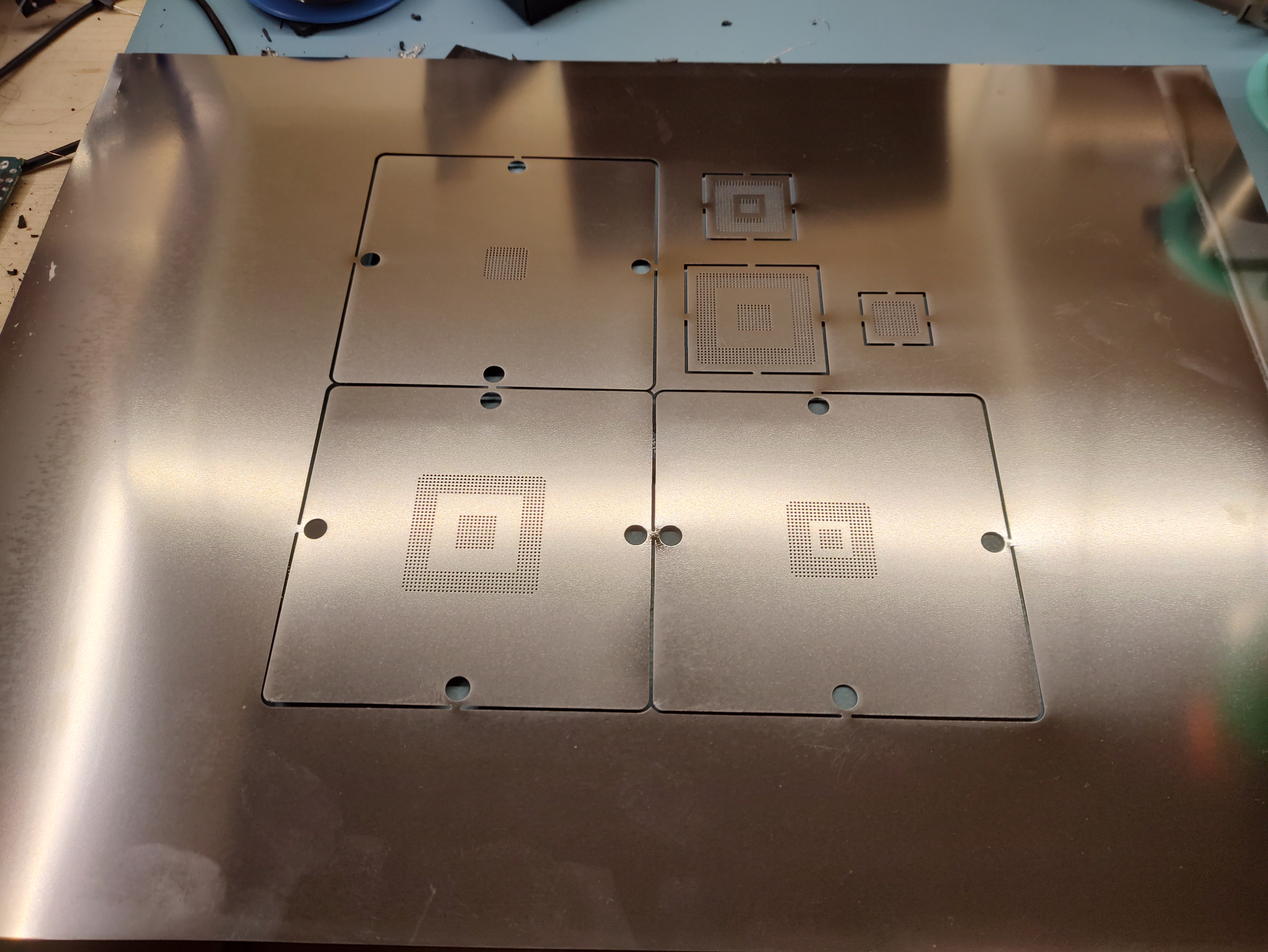
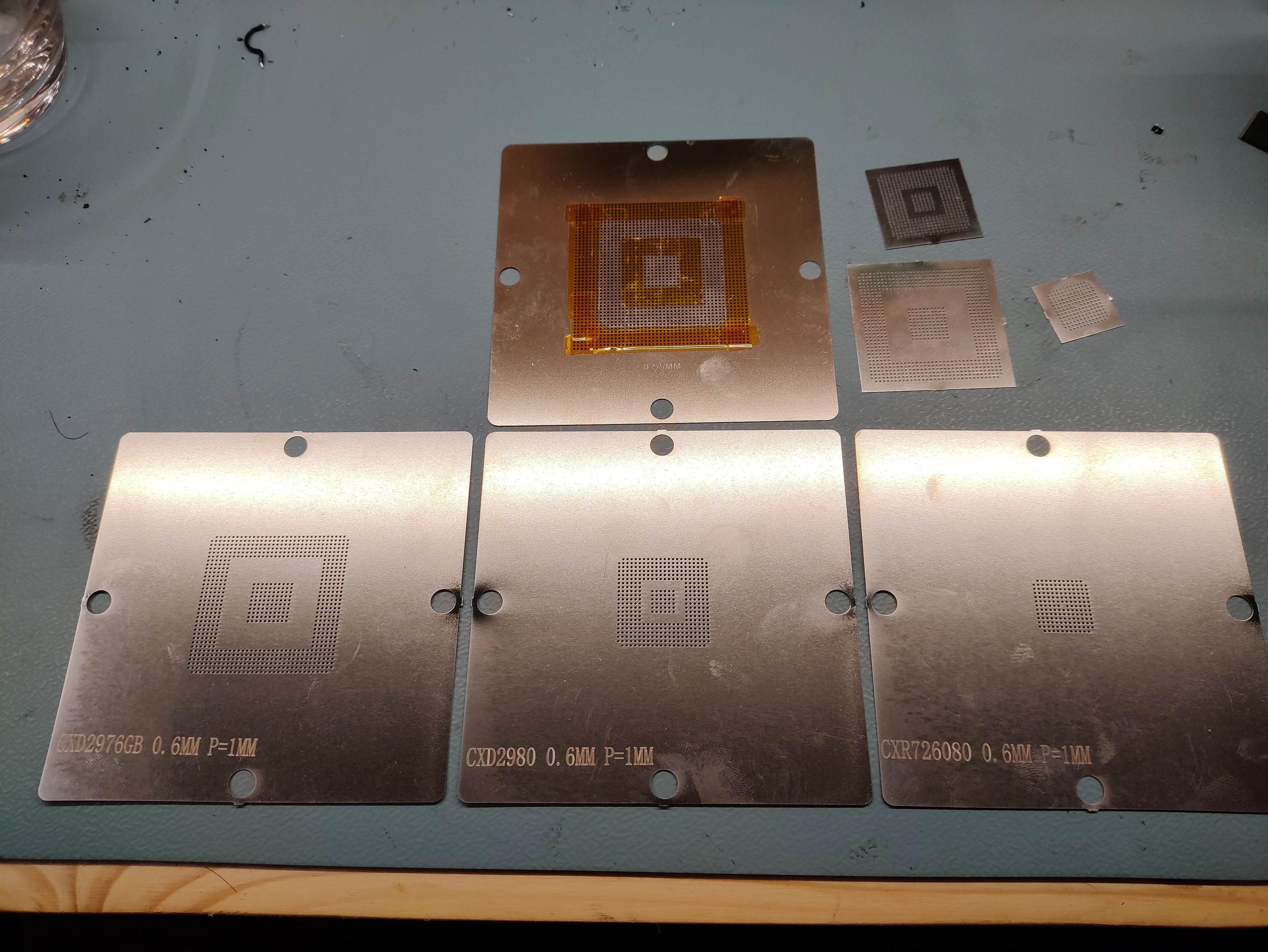
I'm slowly preparing for the next mainboard revision and for that I needed some reballing stencils for the EE, GS and Mechacon. Last time I had to use one universal stencil for all chips and mask the unused pads with kapton tape, but I'm not willing to go through that waste of time again.
I was searching for commercial stencils that fit my reballing fixture for a while now and couldn't find any, so I designed my own. As I already have the footprints, it was just a matter of adjusting the paste expansion and drawing the outlines. I designed the stencils to fit within the valid area of JLCs smallest (and cheapest) SMT stencil size(190x290mm). Engraving was pretty cheap too, so I even added the part numbers of the chips. The ideal thickness of the stencils would be 0.25mm, but JLC only offers 0.2 or 0.3mm with 0.3mm being more expensive.
I decided to go cheap by specifying the 0.2mm thickness, but in the end JLC delivered 0.15mm stencils, that's something to be aware of. The stability with 0.15mm should be fine, but maybe it's a bit trickier to adjust the ideal height over the BGA.
In case someone can find them useful, I've attached the layout file and the Gerbers I used for ordering. The cutouts are optimized for 0.5mm or 0.55mm solder balls. I haven't tried reballing, but I've test-fitted all stencils on the actual chips. The files contain a panel outline too, so the panel can either have a 190x190mm custom size or JLCs default 380x280mm stencil size. Even though shipping is more expensive I chose the latter, because I can make use of the excess sheet metal.
For ordering I included the following comments:
-Please do not change the stencil aperture
-Stencil thickness: 0.2mm
-Engraving: Text and position, see file "engrave.gbr"
Memory Card:
I came to the decision that I would like to use my reverse engineered SD-card sized memory cards for my portable to reduce the size. The portable will most likely have both memory card slots exposed and together with that comes one difficulty: the system has to differentiate between a normal SD card (MX4SIO) and the memory SD card. The main difference is that the MX4SIO requires the ACK to be pulled low, as a standard SD card doesn't have that signal. For fixing this I modified a MX4SIO memory card to connect ACK (it is using DAT2/pin9 as ACK) when a memory card is plugged and to pull ACK down when an SD card is plugged. I'm doing this using a simple little analog switch, which is toggled using the WRITE_PROTECT pin of the SD card socket. If a card is write protected, it enters memory card mode (connect ACK); if a card is unprotected, it enters MX4SIO mode (pull ACK down). Here is the circuit:
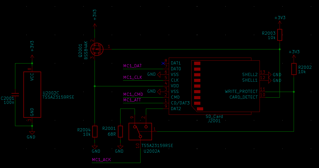
I'm happy with the results and will continue using this circuit.
Gamepad:
There were some things to take into account before designing anything:
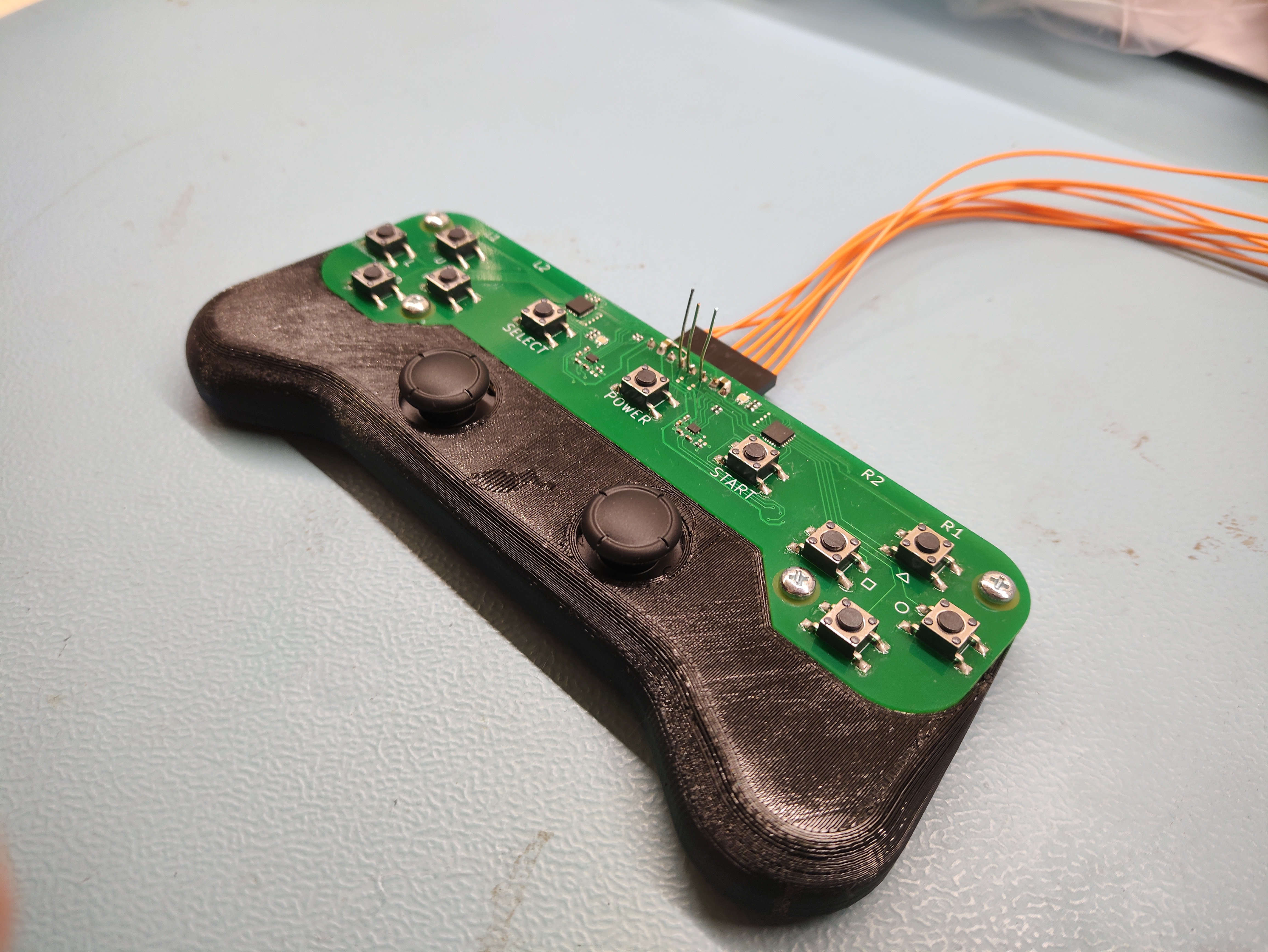
The gamepad prototype was designed and ordered and I even had some time left to start writing the drivers for the I2C devices before my vacation. Currently there is one IO expander and one ADC per gamepad side, so I have 32 IO channels and 4 analog channels in total. The prototype is using some of the 16 unused channels as simple LED outputs, but I could also add extra buttons (volume, brightness?). I included the power button on the gamepad prototype too.
For the analog sticks I want to use the GuliKit hall effect joycon joysticks, that gives me one restriction right now: as far as I know, the joycons are running at 1.8V and I assume the hall analog sticks are also only rated for that voltage.
I could not find any specifications for them, so I created a support ticket at GuliKit to get the operating voltage range of the sticks (because they do contain active circuitry). For now the analog section of the gamepad prototype is running on 1.8V, with the option to switch to 3.3V. I haven't heard back from GuliKit and if they keep ignoring my request, I may have to risk destroying 2 joysticks for science. If I don't need 1.8V there would be only 6 connections for the gamepad: 3.3V, GND, SDA, SCL, INT(not used currently), RESET.
Here's my new toy, maybe a bit too fancy for a development prototype:
Next up was writing the code for emulating a DS2 controller. The DS2 protocol logic was straight forward to implement due to the many reverse engineering resources online, but the SPI part was driving me nuts for a couple of evenings. My main problem was that in the RP2040 I couldn't find a proper interrupt that triggers when there is one byte in the SPI RX FIFO, only one that triggers when the FIFO is half-full.
So the next idea was to poll the SPI using the blocking SPI functions. That caused lots of problems, because those functions read and write a byte at the same time. It means that I had to write a response into the TX buffer before processing the command, which would especially cause problems in the last byte of a transmission, where I shouldn't write anything into the TX buffer. When I did, all TX byted afterwards were shifted by 1. Because of that I included an interrupt for falling/rising edges on the ATT line to reset the SPI peripheral after each transmission, which solved the byte shifting issue. Maybe someone knows how to reset only the FIFO?
Due to the blocking function I did not have enough time to process the commands either, which caused the gamepad to miss some bytes, especially when filling the response buffer after the second CMD byte. I solved this by removing the SPI read function altogether and polling the FIFO status bit directly to read a byte. It means that I can read the command, process the data, and afterwards determine whether or what to write into the TX FIFO. I saw that there would be an interrupt to trigger a DMA transfer to achieve something similar, but I didn't try yet.
Another problem was that the DATA signal is supposed to be floating between transmissions, the RP2040 SPI peripheral doesn't support that as far as I can tell. I had to cheat a little by overriding the output buffer of the SPI TX pin during the ATT rising edge and setting it back to SPI during the ATT falling edge. It only leaves one glitch while resetting the SPI where the DATA would go LOW for a couple of microseconds, but it doesn't seem to interfere with normal operation.
At that point I got the gamepad 80% working, but there were still timing issues with the ACK signal. The ACK is supposed to happen after every byte and it was still generated by a blocking function using sleep_us(), which 1) had very inconsistent timing and 2) sometimes caused the logic to miss bytes. Now it is generated by a timer interrupt, which is more consistent.
Using this implementation the gamepad works pretty well in all games I've tested so far. And I didn't mention it yet: the whole gamepad code is running on core1 of the RP2040, so the normal operation of the Syscon is not affected at all. Reading the button states is still the responsibility of core0 right now, mainly because the gamepad is connected to the same I2C as the power management and I wanted to avoid conflicts between the cores when accessing the I2C.
I tried to make the gamepad code as flexible as possible, allowing button and analog stick remapping & inverting on the fly. I also left the option to fill the button pressure response with something other that 0x00 and 0xFF (maybe analog buttons one day?).
What's missing still is the polling response configuration (command 0x4F), right now all polling responses are always enabled, regardless of what the PS2 configures (which could cause non-functional pressure responses in some games).
The next thing to implement is an analog stick calibration function. All analog stick parameters can be changed at any time (min, max, center, deadzone) and are remapped to 0x00-0xFF, but I have no function to actually calibrate them. The current calibration was done manually by writing the min&max I measured into the initialization.
Then there is one last timing bug to troubleshoot: sometimes (random; ~ every couple minutes?) there are ghost inputs. I have some theories already, but I need to do more testing to find what exactly causes it. Right now, contention between the two cores is my main suspect (both are accessing the same struct for operation and for reading/writing button states)
Edit: here is a small and shitty demonstration of the gamepad:
During testing I also discovered a couple other things to fix and implement next:
It's summertime, so priorities depend on motivation, time budget and weather

This time there is not as much progress as I was on vacation, but I'm pretty happy with the things I was able to achieve:
Mainboard:
I'm slowly preparing for the next mainboard revision and for that I needed some reballing stencils for the EE, GS and Mechacon. Last time I had to use one universal stencil for all chips and mask the unused pads with kapton tape, but I'm not willing to go through that waste of time again.
I was searching for commercial stencils that fit my reballing fixture for a while now and couldn't find any, so I designed my own. As I already have the footprints, it was just a matter of adjusting the paste expansion and drawing the outlines. I designed the stencils to fit within the valid area of JLCs smallest (and cheapest) SMT stencil size(190x290mm). Engraving was pretty cheap too, so I even added the part numbers of the chips. The ideal thickness of the stencils would be 0.25mm, but JLC only offers 0.2 or 0.3mm with 0.3mm being more expensive.
I decided to go cheap by specifying the 0.2mm thickness, but in the end JLC delivered 0.15mm stencils, that's something to be aware of. The stability with 0.15mm should be fine, but maybe it's a bit trickier to adjust the ideal height over the BGA.
In case someone can find them useful, I've attached the layout file and the Gerbers I used for ordering. The cutouts are optimized for 0.5mm or 0.55mm solder balls. I haven't tried reballing, but I've test-fitted all stencils on the actual chips. The files contain a panel outline too, so the panel can either have a 190x190mm custom size or JLCs default 380x280mm stencil size. Even though shipping is more expensive I chose the latter, because I can make use of the excess sheet metal.
For ordering I included the following comments:
-Please do not change the stencil aperture
-Stencil thickness: 0.2mm
-Engraving: Text and position, see file "engrave.gbr"
Memory Card:
I came to the decision that I would like to use my reverse engineered SD-card sized memory cards for my portable to reduce the size. The portable will most likely have both memory card slots exposed and together with that comes one difficulty: the system has to differentiate between a normal SD card (MX4SIO) and the memory SD card. The main difference is that the MX4SIO requires the ACK to be pulled low, as a standard SD card doesn't have that signal. For fixing this I modified a MX4SIO memory card to connect ACK (it is using DAT2/pin9 as ACK) when a memory card is plugged and to pull ACK down when an SD card is plugged. I'm doing this using a simple little analog switch, which is toggled using the WRITE_PROTECT pin of the SD card socket. If a card is write protected, it enters memory card mode (connect ACK); if a card is unprotected, it enters MX4SIO mode (pull ACK down). Here is the circuit:
I'm happy with the results and will continue using this circuit.
Gamepad:
There were some things to take into account before designing anything:
- The first question was: how to interface with the user inputs? The main problem is that the Syscon doesn't have enough IO left to read all user inputs.
- The second thought: In the portable I would like to split the left and right gamepad sections from the mainboard, so they will most likely require a ffc connection. I2C would be perfect to reduce the amount of lines and to solve the lack of GPIOs, while providing the flexibility to add whatever I want to the gamepad hardware.
The gamepad prototype was designed and ordered and I even had some time left to start writing the drivers for the I2C devices before my vacation. Currently there is one IO expander and one ADC per gamepad side, so I have 32 IO channels and 4 analog channels in total. The prototype is using some of the 16 unused channels as simple LED outputs, but I could also add extra buttons (volume, brightness?). I included the power button on the gamepad prototype too.
For the analog sticks I want to use the GuliKit hall effect joycon joysticks, that gives me one restriction right now: as far as I know, the joycons are running at 1.8V and I assume the hall analog sticks are also only rated for that voltage.
I could not find any specifications for them, so I created a support ticket at GuliKit to get the operating voltage range of the sticks (because they do contain active circuitry). For now the analog section of the gamepad prototype is running on 1.8V, with the option to switch to 3.3V. I haven't heard back from GuliKit and if they keep ignoring my request, I may have to risk destroying 2 joysticks for science. If I don't need 1.8V there would be only 6 connections for the gamepad: 3.3V, GND, SDA, SCL, INT(not used currently), RESET.
Here's my new toy, maybe a bit too fancy for a development prototype:
Next up was writing the code for emulating a DS2 controller. The DS2 protocol logic was straight forward to implement due to the many reverse engineering resources online, but the SPI part was driving me nuts for a couple of evenings. My main problem was that in the RP2040 I couldn't find a proper interrupt that triggers when there is one byte in the SPI RX FIFO, only one that triggers when the FIFO is half-full.
So the next idea was to poll the SPI using the blocking SPI functions. That caused lots of problems, because those functions read and write a byte at the same time. It means that I had to write a response into the TX buffer before processing the command, which would especially cause problems in the last byte of a transmission, where I shouldn't write anything into the TX buffer. When I did, all TX byted afterwards were shifted by 1. Because of that I included an interrupt for falling/rising edges on the ATT line to reset the SPI peripheral after each transmission, which solved the byte shifting issue. Maybe someone knows how to reset only the FIFO?
Due to the blocking function I did not have enough time to process the commands either, which caused the gamepad to miss some bytes, especially when filling the response buffer after the second CMD byte. I solved this by removing the SPI read function altogether and polling the FIFO status bit directly to read a byte. It means that I can read the command, process the data, and afterwards determine whether or what to write into the TX FIFO. I saw that there would be an interrupt to trigger a DMA transfer to achieve something similar, but I didn't try yet.
Another problem was that the DATA signal is supposed to be floating between transmissions, the RP2040 SPI peripheral doesn't support that as far as I can tell. I had to cheat a little by overriding the output buffer of the SPI TX pin during the ATT rising edge and setting it back to SPI during the ATT falling edge. It only leaves one glitch while resetting the SPI where the DATA would go LOW for a couple of microseconds, but it doesn't seem to interfere with normal operation.
At that point I got the gamepad 80% working, but there were still timing issues with the ACK signal. The ACK is supposed to happen after every byte and it was still generated by a blocking function using sleep_us(), which 1) had very inconsistent timing and 2) sometimes caused the logic to miss bytes. Now it is generated by a timer interrupt, which is more consistent.
Using this implementation the gamepad works pretty well in all games I've tested so far. And I didn't mention it yet: the whole gamepad code is running on core1 of the RP2040, so the normal operation of the Syscon is not affected at all. Reading the button states is still the responsibility of core0 right now, mainly because the gamepad is connected to the same I2C as the power management and I wanted to avoid conflicts between the cores when accessing the I2C.
I tried to make the gamepad code as flexible as possible, allowing button and analog stick remapping & inverting on the fly. I also left the option to fill the button pressure response with something other that 0x00 and 0xFF (maybe analog buttons one day?).
What's missing still is the polling response configuration (command 0x4F), right now all polling responses are always enabled, regardless of what the PS2 configures (which could cause non-functional pressure responses in some games).
The next thing to implement is an analog stick calibration function. All analog stick parameters can be changed at any time (min, max, center, deadzone) and are remapped to 0x00-0xFF, but I have no function to actually calibrate them. The current calibration was done manually by writing the min&max I measured into the initialization.
Then there is one last timing bug to troubleshoot: sometimes (random; ~ every couple minutes?) there are ghost inputs. I have some theories already, but I need to do more testing to find what exactly causes it. Right now, contention between the two cores is my main suspect (both are accessing the same struct for operation and for reading/writing button states)
Edit: here is a small and shitty demonstration of the gamepad:
During testing I also discovered a couple other things to fix and implement next:
- Battery SOC tracking, warning and shutoff; the Syscon is only printing the SOC currently, but not doing anything with it. It happened already that the SOC reached 0%, the MAX17320 entered BATLOW protection and disconnected the battery. That leads to the next issue I discovered:
- The Syscon currently has no implementation to recover from such faults; in the error above I have to unplug and replug the battery to get the system working again, while it would be easy to fix by clearing the fault bits of the MAX17320
- Another thing that most likely broke during refactoring: the system always limits the charge current to 500mA, I think I changed some settings in the BQ25792 that I should revert
- implement the missing gamepad functions and debug the remaining timing issues + code cleanup
- implement the missing functions in the power management for error handling and SOC; fix the charging bug
- look into designing a shield for my FPGA development board to finally start messing with video and audio
It's summertime, so priorities depend on motivation, time budget and weather
Attachments
-
615.9 KB Views: 59
Last edited:
thedrew
.
- Joined
- Sep 27, 2016
- Messages
- 416
- Likes
- 896
Really interesting update and fantastic progress as usual! Always a joy to read. I'm using some hall sticks from a retro handheld (Retroid Pocket 3) for a couple projects of mine as well and they are running on 3.3v. I think this would be a good choice for you so you can just use 3.3v across the board on your custom controller board and not have to worry about the 1.8v the GuliKit uses. The caps of these sticks are a little bit smaller than the Switch sticks, but I think it is nice for a change. You can see a comparison pic between the Retroid Pocket 3 hall stick vs the regular Switch stick at the bottom of my post here from my PS2 worklog:
https://bitbuilt.net/forums/index.php?threads/vs2-worklog.5303/post-56742
And you can get the hall sticks that run off 3.3v here:
https://www.goretroid.com/collections/diy/products/retroid-pocket-3-3-handheld-console-hall-joystick
https://bitbuilt.net/forums/index.php?threads/vs2-worklog.5303/post-56742
And you can get the hall sticks that run off 3.3v here:
https://www.goretroid.com/collections/diy/products/retroid-pocket-3-3-handheld-console-hall-joystick
I can confirm the Gulikit sticks work on 1V8 only. Do not give them 3V3 or 5V or you will destroy them (as I did).
Tschicki
.
Really interesting update and fantastic progress as usual! Always a joy to read. I'm using some hall sticks from a retro handheld (Retroid Pocket 3) for a couple projects of mine as well and they are running on 3.3v. I think this would be a good choice for you so you can just use 3.3v across the board on your custom controller board and not have to worry about the 1.8v the GuliKit uses. The caps of these sticks are a little bit smaller than the Switch sticks, but I think it is nice for a change. You can see a comparison pic between the Retroid Pocket 3 hall stick vs the regular Switch stick at the bottom of my post here from my PS2 worklog:
https://bitbuilt.net/forums/index.php?threads/vs2-worklog.5303/post-56742
And you can get the hall sticks that run off 3.3v here:
https://www.goretroid.com/collections/diy/products/retroid-pocket-3-3-handheld-console-hall-joystick
Thanks for the confirmation!I can confirm the Gulikit sticks work on 1V8 only. Do not give them 3V3 or 5V or you will destroy them (as I did).
The Retroid analog sticks look interesting too, I've ordered a set for comparison. They should even fit my prototye, assuming everything but the caps is identical to the switch sticks. For now both seem to have pros and cons. I feel like I prefer the swappable&bigger stick caps of the Gulikit design + the availability, but the 3.3V operating voltage of the Retroid sticks would save me either an LDO or an additional line to the mainboard (right now the 1.8V comes from the PS2 1V8 rail, so no analog sticks while the PS2 is off).
I will decide when I get them and will keep you updated!
Tschicki
.
Time for a small update!
I spent the last month mainly on integrating all circuits I made so far and working out how to best implement the video processor.
Let's start with the system integration...
My old modular setup with all the interconnects and hand-soldered wiring was starting to develop connectivity issues after getting pushed around on my desk for a couple of months. The main concern was the pin headers for powering the custom mainboard - the console crashed very often when I started moving the setup. Another issue was my fire hazard of a battery setup with the janky pin headers and the exposed traces...
In order to fix those issues and to start a first proof-of-concept for my portable, I combined the circuits with all my findings and improvements into one single 4 layer board (with impedance control for USB). Now you can also start to see why I chose this form factor for the first mainboard, why it has threaded M2 standoffs and why all FFC sockets are convenientely located around the edges. The new board is stacked below the mainboard and connected via short FFC (PS2 power has direct solder connections). The layout was a bit awkward, as I had to adapt to what was already there, but it should do the job just fine. It should be much more robust for testing and development now. The new board includes:
I assembled one board already and did some testing (you can tell by all the bodge wires). Not proud of all the bodges, I think i rushed this one a bit too much - now it works as intended though.
An issue I noticed during testing makes manufacturing unneccessarily hard. The first thing to do after assembly is to write the configs into the NVM of the STUSB4500 and the MAX17320. This requires the syscon to power up in order to flash the FW and to run the setup functions. My problem was that the soft power switch needs VRTC to power on the system. VRTC is generated by the MAX17320, but it doesn't do that by default - you need to program it first.
My intended configuration process was this:
The next issue was that the pinouts of the SD card slots were flipped, so I had to manually fix them. Would have been so easy to crosscheck with the actual SD card...
When it came to testing the audio I had a lot of issues too...
The code to control the LM49450 was simple to implement, I got the configs from the U-Amp and it's only a couple of registers to write. But the power supplies on the other hand were causing lots of issues. I was already a bit sceptical while doing the schematics, because the DDS was very vague on powering the chip and power sequencing.
My intention was that the LM49450 is entirely powered by the PS2, so 3.3V (digital core, IO), 5V (gain stage and sp output driver), 2.5V (hp). BUT - the chip pulls SDA and SCL low when unpowered, blocking the power management I2C and preventing the system from booting.
Plan B was to power the digital core and IO from the syscon 3.3V and powering the remaining power pins together with the PS2. This did work, the I2C was not blocked and you can even set the registers with only the core and IO powered, BUT the LM49450 was back-powering the PS2 5V rail. I realized it pretty quickly when the LM49450 was getting blazing hot while the (unpowered) 5V fan was spinning...
So for now everything but the headphone supply is powered by the syscon 3.3V. The headphone supply is still connected to the PS2 2.5V, but it doesn't seem to cause issues. I will think about more elegant ways to power the LM49450 for the next revision.
There was another little design oversight regarding the headphone sense pin, I simply forgot to connect it to the syscon. That made it impossible to differentiate between speaker volume and headphone volume, so I had to connect that signal manually. It didn't seem to work in the beginning, the LM49450 was only outputting audio on the speakers as soon as the syscon was connected to the HPS pin. After checking it was clear that the syscon input pin was loading the HPS down to a couple 100mV with plugged headphones - seems like the LM49450 only has some very weak pullup on HPS.
That one was interesting to figure out... did you know that the RP2040 has pulldowns enabled on all inputs by default? You have to actively turn them off during the initialization. The more you know....
After fixing the initialization in FW I had a happy LM49450 doing exactly what it's supposed to do. Speakers and headphones are working and I even implemented a crude function to change the speaker or headphone volume. A happy end after all, but it took longer than it should have...
To check the stability I had some intense gaming sessions the last two evenings and it works great so far! It's just too tempting to play some GTA instead of developing when the setup is sitting right next to the keyboard...
Analog Sticks...
Another thing I was working on were the analog sticks. As I'm planning to use switch-style hall effect sticks, my first choice were the Gulikit sticks. The problem is that they only run from 1.8V and everything else is running from 3.3V, it would require either an additional LDO or another line to the controller boards. I got the Retroid hall effect sticks as suggested by @thedrew to do a couple of tests and I have to say that mechanically they feel much better than the Gulikit ones (while being much cheaper...). I was surprised that the smaller caps actually feel better and they have a better grip too.
My only issue so far is that I cannot get them to work properly electrically. They don't drift, that's not the issue, but even after basic calibration the diagonal directions are way off. They essentially feel like a dpad, with the diagonals outputting smaller values to the point of it being annoying during gameplay. It's almost like their output is not linear and I couldn't find a proper algorithm yet to compensate for it. Maybe someone has an idea?
At this point I have the functionality of most circuits kinda proven & working, except for one thing... Video!
The last task I started this month is to develop the video processor. This one will take some time, as it's my first (proper) project on an FPGA. We did some VHDL in the past, but mostly simulation, so this one will be a lot of fun and a lot to learn. Exciting!
The FPGA of choice is the Artix-7 A35, because I already have the development board. Not happy with the price point, I will consider switching to something else when I have a working implementation. Efinix have some pretty interesting (and cheap) FPGAs....and I saw that the Retro Gem is using one too (Trion T20)
But before programming anything I had to set some preliminary goals I want to achieve:
I'm already working on an interface board to plug into my mainboard, it will contain my Alchitry Au, video input FFC, 40 pin display FFC and a backlight driver. The pin headers on both sides are for my 32CH logic analyzer, that way I can observe the input and output video stream for debugging.
Unfortunately the Alchitry Au can only support up to 20 1.8V logic level signals, which is not enough for my application. For now I had to include high speed SN74AVC8T245 bus transceivers between the video input and the development board to shift the signals up to 3.3V.
I also spent some time thinking about how to interface between the syscon and the FPGA. Ideally I would like to write into the output framebuffer to display battery levels and maybe even have a little menu (terminal-style). For that I already reserved a full SPI connection on the new integrated power management board (the unconnected FFC socket above). That way I could implement some simple SPI slave in the FPGA to accept a couple of commands. The bandwidth should be there as the SPI can go up to ~60MHz, it should be plenty to write a couple of sprites into the framebuffer.
Here is the current state of the board, it's very early in the design process and a lot will change:
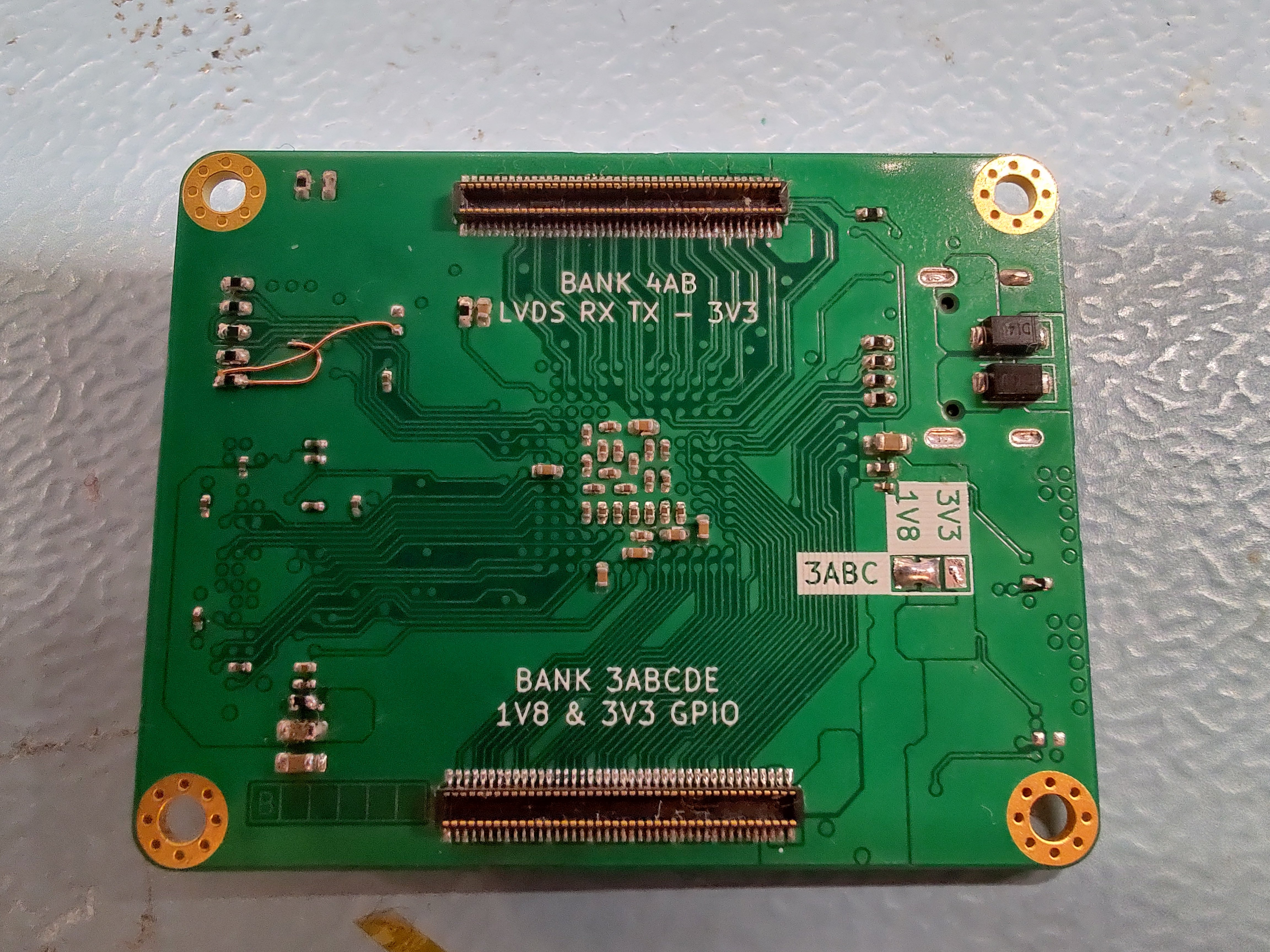
In parallel I'm tinkering with vivado, the IO planning for the above board is done already. I hooked up the (not yet)1.8V and 3.3V signals to two different neighboring banks, in case I want to create a custom board using this FPGA (without changing the pinout too much).
The first function to implement will probably be the DPI video output for the display. Next would be the video input and when both are working I will do the deinterlacing and scaling (that will be fun, especially handling the framebuffers to avoid conflicts).
That's it for now, will keep you updated!
I spent the last month mainly on integrating all circuits I made so far and working out how to best implement the video processor.
Let's start with the system integration...
My old modular setup with all the interconnects and hand-soldered wiring was starting to develop connectivity issues after getting pushed around on my desk for a couple of months. The main concern was the pin headers for powering the custom mainboard - the console crashed very often when I started moving the setup. Another issue was my fire hazard of a battery setup with the janky pin headers and the exposed traces...
In order to fix those issues and to start a first proof-of-concept for my portable, I combined the circuits with all my findings and improvements into one single 4 layer board (with impedance control for USB). Now you can also start to see why I chose this form factor for the first mainboard, why it has threaded M2 standoffs and why all FFC sockets are convenientely located around the edges. The new board is stacked below the mainboard and connected via short FFC (PS2 power has direct solder connections). The layout was a bit awkward, as I had to adapt to what was already there, but it should do the job just fine. It should be much more robust for testing and development now. The new board includes:
- an improved battery management circuit
- the BQ25792 now has a shipfet populated to enable overdischarge-current protection on the charger side
- all mosfets in the battery current path were upgraded from 10Apk to 60Apk (seriously, I want them to be the last thing to fail, as they usually fail closed)
- the soft power circuit was simplified
- the USB C now has proper ESD protection on all used signals
- streamlined power management
- the buck converter circuits were simplified to reduce component count (the TPS629210 output voltage can be set via a single resistor); 1V25 is now 1V and 3V5 is now 3.3V permanently
- 2V5 and 1V8 are now handled by a single fixed LDO with two outputs; it's cheaper than 2 separate LDOs with feedback resistors
- all PG are tied together and connected to the syscon to detect faults
- integrated RP2040
- it now has 2 separate I2C for power management and the gamepad circuitry; I'm planning to do everything gamepad related in core1 and to avoid conflicts on the I2C (and additional work...) they are split now
- SWD and UART headers as before
- the USB of the pico is connected to the USB C for easy firmware upgrades (haven't tested it yet though)
- integrated I2S audio using LM49450
- contains all IO I intend to have in my portable
- 2 SD memory card slots; both can auto-detect MX4SIO and my custom SD sized memory card
- 1 USB; now has a load switch with current limit on the 5V
- stereo headphone jack, switching between speakers and headphones
- 2 speaker outputs
- 1 fan output with PWM control (by syscon)
I assembled one board already and did some testing (you can tell by all the bodge wires
). Not proud of all the bodges, I think i rushed this one a bit too much - now it works as intended though.An issue I noticed during testing makes manufacturing unneccessarily hard. The first thing to do after assembly is to write the configs into the NVM of the STUSB4500 and the MAX17320. This requires the syscon to power up in order to flash the FW and to run the setup functions. My problem was that the soft power switch needs VRTC to power on the system. VRTC is generated by the MAX17320, but it doesn't do that by default - you need to program it first.
My intended configuration process was this:
- plug in a battery
- plug in a charger to start the syscon
- flash the FW to write the NVM
- run the FW while pressing the power button to flash the NVM
- flash the default FW and run it
- unplug the charger and press the power button to boot
The next issue was that the pinouts of the SD card slots were flipped, so I had to manually fix them. Would have been so easy to crosscheck with the actual SD card...
When it came to testing the audio I had a lot of issues too...
The code to control the LM49450 was simple to implement, I got the configs from the U-Amp and it's only a couple of registers to write. But the power supplies on the other hand were causing lots of issues. I was already a bit sceptical while doing the schematics, because the DDS was very vague on powering the chip and power sequencing.
My intention was that the LM49450 is entirely powered by the PS2, so 3.3V (digital core, IO), 5V (gain stage and sp output driver), 2.5V (hp). BUT - the chip pulls SDA and SCL low when unpowered, blocking the power management I2C and preventing the system from booting.
Plan B was to power the digital core and IO from the syscon 3.3V and powering the remaining power pins together with the PS2. This did work, the I2C was not blocked and you can even set the registers with only the core and IO powered, BUT the LM49450 was back-powering the PS2 5V rail. I realized it pretty quickly when the LM49450 was getting blazing hot while the (unpowered) 5V fan was spinning...
So for now everything but the headphone supply is powered by the syscon 3.3V. The headphone supply is still connected to the PS2 2.5V, but it doesn't seem to cause issues. I will think about more elegant ways to power the LM49450 for the next revision.
There was another little design oversight regarding the headphone sense pin, I simply forgot to connect it to the syscon. That made it impossible to differentiate between speaker volume and headphone volume, so I had to connect that signal manually. It didn't seem to work in the beginning, the LM49450 was only outputting audio on the speakers as soon as the syscon was connected to the HPS pin. After checking it was clear that the syscon input pin was loading the HPS down to a couple 100mV with plugged headphones - seems like the LM49450 only has some very weak pullup on HPS.
That one was interesting to figure out... did you know that the RP2040 has pulldowns enabled on all inputs by default? You have to actively turn them off during the initialization. The more you know....
After fixing the initialization in FW I had a happy LM49450 doing exactly what it's supposed to do. Speakers and headphones are working and I even implemented a crude function to change the speaker or headphone volume. A happy end after all, but it took longer than it should have...
To check the stability I had some intense gaming sessions the last two evenings and it works great so far! It's just too tempting to play some GTA instead of developing when the setup is sitting right next to the keyboard...
Analog Sticks...
Another thing I was working on were the analog sticks. As I'm planning to use switch-style hall effect sticks, my first choice were the Gulikit sticks. The problem is that they only run from 1.8V and everything else is running from 3.3V, it would require either an additional LDO or another line to the controller boards. I got the Retroid hall effect sticks as suggested by @thedrew to do a couple of tests and I have to say that mechanically they feel much better than the Gulikit ones (while being much cheaper...). I was surprised that the smaller caps actually feel better and they have a better grip too.
My only issue so far is that I cannot get them to work properly electrically. They don't drift, that's not the issue, but even after basic calibration the diagonal directions are way off. They essentially feel like a dpad, with the diagonals outputting smaller values to the point of it being annoying during gameplay. It's almost like their output is not linear and I couldn't find a proper algorithm yet to compensate for it. Maybe someone has an idea?
At this point I have the functionality of most circuits kinda proven & working, except for one thing... Video!
The last task I started this month is to develop the video processor. This one will take some time, as it's my first (proper) project on an FPGA. We did some VHDL in the past, but mostly simulation, so this one will be a lot of fun and a lot to learn. Exciting!
The FPGA of choice is the Artix-7 A35, because I already have the development board. Not happy with the price point, I will consider switching to something else when I have a working implementation. Efinix have some pretty interesting (and cheap) FPGAs....and I saw that the Retro Gem is using one too (Trion T20)
But before programming anything I had to set some preliminary goals I want to achieve:
- parallel RGB video input from the GS
- support for progressive and interlaced inputs and multiple resolutions (PAL and NTSC)
- weave deinterlacing (something more advanced like motion-adaptive is way outside my capabilities)
- bilinear up and down scaling; it shall adapt to input resolution changes automatically
- DPI video output to drive a generic 5 inch 480p IPS
- a way to write system information into the framebuffer
I'm already working on an interface board to plug into my mainboard, it will contain my Alchitry Au, video input FFC, 40 pin display FFC and a backlight driver. The pin headers on both sides are for my 32CH logic analyzer, that way I can observe the input and output video stream for debugging.
Unfortunately the Alchitry Au can only support up to 20 1.8V logic level signals, which is not enough for my application. For now I had to include high speed SN74AVC8T245 bus transceivers between the video input and the development board to shift the signals up to 3.3V.
I also spent some time thinking about how to interface between the syscon and the FPGA. Ideally I would like to write into the output framebuffer to display battery levels and maybe even have a little menu (terminal-style). For that I already reserved a full SPI connection on the new integrated power management board (the unconnected FFC socket above). That way I could implement some simple SPI slave in the FPGA to accept a couple of commands. The bandwidth should be there as the SPI can go up to ~60MHz, it should be plenty to write a couple of sprites into the framebuffer.
Here is the current state of the board, it's very early in the design process and a lot will change:
In parallel I'm tinkering with vivado, the IO planning for the above board is done already. I hooked up the (not yet)1.8V and 3.3V signals to two different neighboring banks, in case I want to create a custom board using this FPGA (without changing the pinout too much).
The first function to implement will probably be the DPI video output for the display. Next would be the video input and when both are working I will do the deinterlacing and scaling (that will be fun, especially handling the framebuffers to avoid conflicts).
That's it for now, will keep you updated!
Tschicki
.
Small update!
The video processor is showing the first signs of life!
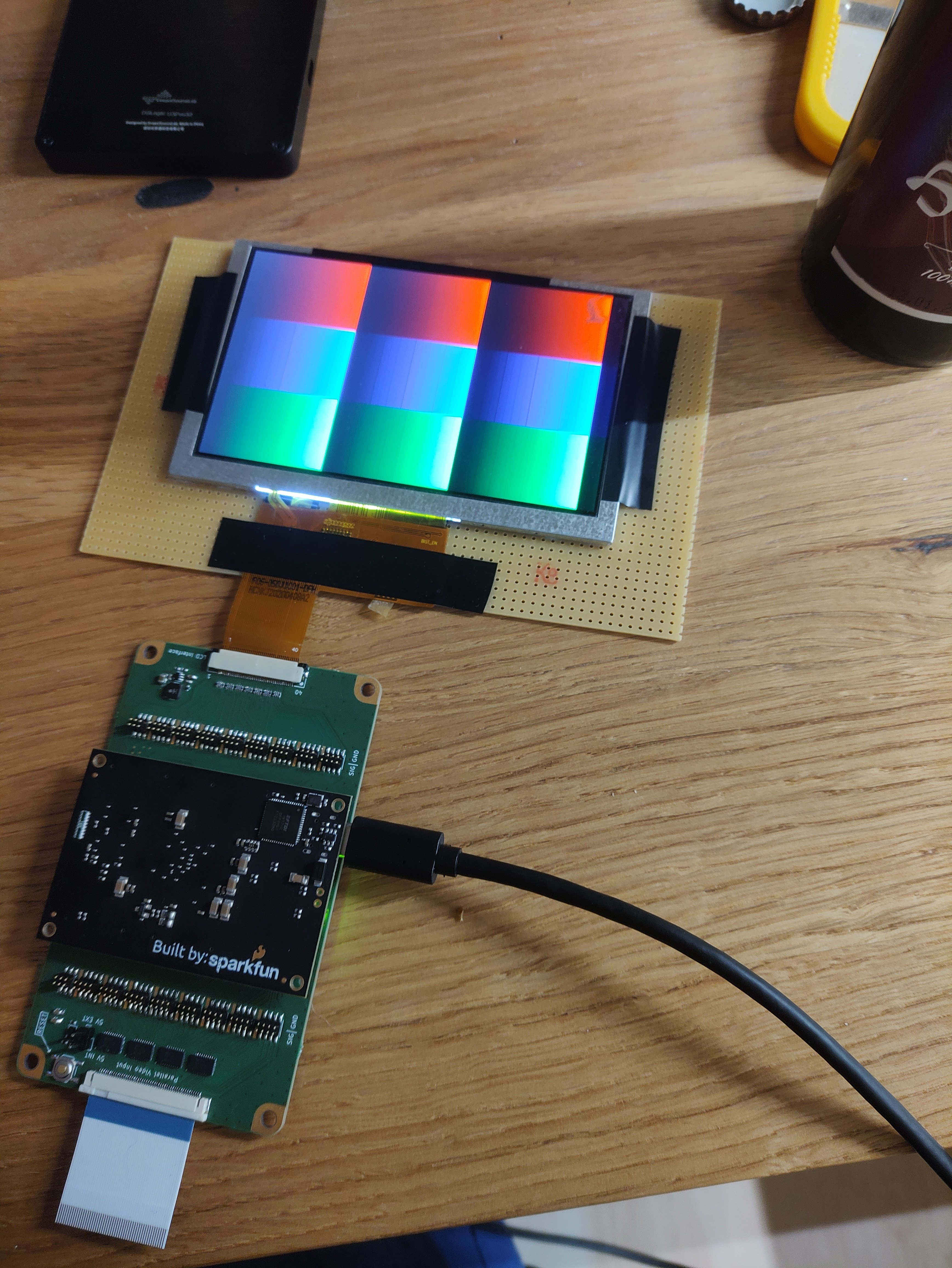
Last week I got the interface board assembled and in the last 2 days I had some time to give it a first try. I managed to create a little project for testing the DPI timings, it's just displaying a static image. The datasheet of the display I'm using was very vague about the input timings, but luckily I found a good reference for the timings online. In case someone is interested, here are the timings I'm using:
Horizontal:
data: 800CLK
back porch: 48CLK
front porch: 0CLK
HSYNC: 40CLK
Vertical:
data: 480 lines
back porch: 3 lines
front porch: 0 lines
VSYNC: 13 lines
The Alchitry Au has a 100MHz oscillator, so I'm just dividing it by 2 for now to get the pixel CLK of 50MHz. All output signals are latched with the falling edge of the pixel CLK.
Red looks good ralready, but with green and blue I can observe some periodic vertical artifacts. Especially green has a vertical line that appears when touching the ffc or the output portion of the board. I suspect either signal integrity issues due to the rather large series resistors I used (only had 68R in my parts bin) or bad solder joints (maybe one or more bad lines, as the artifacts are periodic), so there is some investigation needed. Sadly my scope won't be helpful on this one, as it doesn't have enough bandwidth to give me any meaningful hints about signal integrity. The backlight driver looks functional, it's the TPS92360 for reference.
Next up would be to think about an architecture for the video processor. I have a rough idea already, but I will have to work out the exact block diagram, timings, clocking, ...
Creating a DDR3 controller for the framebuffer will be one of the next blocks to try. It's honestly the first time I work with DDR3 (or DDR memory in general), so there is a lot to learn!
Will keep you up to date when I make some noteworthy progress!
Another thing I did on the firmware side is to integrate the whole gamepad into core1 of the RP2040. Now core1 is completely independent and handles the DS2 protocol, the hardware configuration of the IO expanders & ADCs and the polling of the inputs. That takes almost all realtime processing away from core0 and makes a lot of room again for debug messages and experimentation. Core0 only has to handle the macro inputs (vol. up/down) for now.
It created some issues on core1, mainly because I could not poll the buttons within a frame of the DS2 protocol; it would break the timings (due to the funky SPI peripheral). The current solution is to poll the inputs after each frame (gamepad mode) and to poll the inputs periodically when the PS2 is not communicating. To make this happen I added a timeout alert interrupt that is retriggered with every rising edge of the ATT signal. If there is no ATT signal for 500ms, core1 switches to polling mode, where the inputs are polled every 100ms. That way I can also read the buttons and set the LED outputs when the PS2 is off. As soon as core1 sees another rising edge on ATT, it enters gamepad mode again.
The video processor is showing the first signs of life!
Last week I got the interface board assembled and in the last 2 days I had some time to give it a first try. I managed to create a little project for testing the DPI timings, it's just displaying a static image. The datasheet of the display I'm using was very vague about the input timings, but luckily I found a good reference for the timings online. In case someone is interested, here are the timings I'm using:
Horizontal:
data: 800CLK
back porch: 48CLK
front porch: 0CLK
HSYNC: 40CLK
Vertical:
data: 480 lines
back porch: 3 lines
front porch: 0 lines
VSYNC: 13 lines
The Alchitry Au has a 100MHz oscillator, so I'm just dividing it by 2 for now to get the pixel CLK of 50MHz. All output signals are latched with the falling edge of the pixel CLK.
Red looks good ralready, but with green and blue I can observe some periodic vertical artifacts. Especially green has a vertical line that appears when touching the ffc or the output portion of the board. I suspect either signal integrity issues due to the rather large series resistors I used (only had 68R in my parts bin) or bad solder joints (maybe one or more bad lines, as the artifacts are periodic), so there is some investigation needed. Sadly my scope won't be helpful on this one, as it doesn't have enough bandwidth to give me any meaningful hints about signal integrity. The backlight driver looks functional, it's the TPS92360 for reference.
Next up would be to think about an architecture for the video processor. I have a rough idea already, but I will have to work out the exact block diagram, timings, clocking, ...
Creating a DDR3 controller for the framebuffer will be one of the next blocks to try. It's honestly the first time I work with DDR3 (or DDR memory in general), so there is a lot to learn!
Will keep you up to date when I make some noteworthy progress!
Another thing I did on the firmware side is to integrate the whole gamepad into core1 of the RP2040. Now core1 is completely independent and handles the DS2 protocol, the hardware configuration of the IO expanders & ADCs and the polling of the inputs. That takes almost all realtime processing away from core0 and makes a lot of room again for debug messages and experimentation. Core0 only has to handle the macro inputs (vol. up/down) for now.
It created some issues on core1, mainly because I could not poll the buttons within a frame of the DS2 protocol; it would break the timings (due to the funky SPI peripheral). The current solution is to poll the inputs after each frame (gamepad mode) and to poll the inputs periodically when the PS2 is not communicating. To make this happen I added a timeout alert interrupt that is retriggered with every rising edge of the ATT signal. If there is no ATT signal for 500ms, core1 switches to polling mode, where the inputs are polled every 100ms. That way I can also read the buttons and set the LED outputs when the PS2 is off. As soon as core1 sees another rising edge on ATT, it enters gamepad mode again.
thedrew
.
- Joined
- Sep 27, 2016
- Messages
- 416
- Likes
- 896
Me and another member were looking into driving the 24 bit RGB signal directly as well and I have some measurements that might help. Here is the HS, VS, and pixel clock measurements. I accidentally named HS HV, but just know it's HS haha. These files can be opened using Saleae logic analyzing software. This was measured on a 90001 PS2 on the home screen. Hope this helps!
Attachments
-
213.2 KB Views: 50
Tschicki
.
Thanks! I actually don't have a recording of the signals right now, so this will be a good starting point! CLK, HS and VS should be enough to start defining the general timings, soon I will also need to identify the front/back porch and/or find a data EN signal to properly read the pixel data. A couple weeks back I did a recording of all the GS outputs for a couple frames, but stupid me forgot to save it. Will probably need to redo that soon.Me and another member were looking into driving the 24 bit RGB signal directly as well and I have some measurements that might help. Here is the HS, VS, and pixel clock measurements. I accidentally named HS HV, but just know it's HS haha. These files can be opened using Saleae logic analyzing software. This was measured on a 90001 PS2 on the home screen. Hope this helps!
Based on this it would be interesting to make a "simple" proof of concept using just bob deinterlacing, maybe even without scaling for now. That way I could test the timings and the input buffers without the need for external RAM (because DDR3 makes things -a lot- more difficult). It won't look nice due to the lower vertical resolution and I can imagine there would be quite some screen tearing (at least if I don't manage to synchronize the inputs and outputs), but it would help a lot with testing the blocks/learning.
Tschicki
.
GTA Virtual Boy Edition!
I had a couple hours to play with the FPGA and I think I've managed to get the proof of concept working!
[Attached] are some measurements I did on the PS2 video output, they can be opened with DSView 1.3. The first capture shows the OPL menu with all pixel data in PAL 576i. Because the pixel clock was way too fast for that recording I had to do a second one just for CLK, VSYNC, HSYNC at 500MS/s. Based on that I would say the pixel clock is about 54MHz and and the data is transmitted at ~13.5MHz, which would mean 4x oversampling - for PAL 576i.
The output data to my DPI display needs to be transmitted at about 22MHz to match the 50Hz PAL refresh rate (for the frames to stay synchronized). That's about ~1.6 times of the input data rate, so it required some buffering, even for just sending the image 1:1 to the display. But due to the fact that I can only use Block RAM as framebuffer for now, I can only buffer about 180kBytes at a time, which is just enough to store about half a frame in a single color (96% BRAM utilization, that's exatly what you can see in the picture
).For the sake of simplicity, I'm reading every half-frame, buffer a chunk of it and start sending it to the display. In total it's about 288x800 pixels per frame, the rest is filled with black pixels, so what you see in the picture is just half the vertical resolution. There are some artifacts here and there, because the framebuffer is actually only big enough for 200x800 pixels and I had to do some trickery to avoid conflicts when storing and reading from it, while keeping the frames in sync (did not manage to avoid them all the time...)
Next would be to try and get the DDR3 on my development board working to properly buffer the image, then I can also start experimenting with deinterlacing.
I will also have to start thinking about how to implement 480i/480p support, as right now that just leads to a black screen. The NTPAL pin would be an interesting selector there, because I noticed that it is LOW for PAL and HIGH for NTSC. A RST is also issued by the PS2 whenever the NTPAL pin changes states.
Tschicki
.
Update time!
Sorry, I completely forgot to post updates! (again…)
Ever since the last update I’ve been working on FPGA stuff to get the video output of my mainboard up and running and I guess I’m slowly getting there.
After the little experiments with my DPI LCD I know more or less what to expect when it comes to resolutions and video timings. The big blocker was the lack of memory to buffer at least one field of each frame. It made the bridge between the 2 clocking regions very tricky and at some point it stopped me from progressing with my design.
The next logical step was to look into the available RAM options. First, I wanted to try the DDR3 on my Artix 7 Development board, as it would provide plenty of memory at a sufficient speed.
Getting DDR3 working is not trivial, though. I figured that out the hard way after 2 evenings of fighting with vivado’s memory interface generator IP. That “experience” forced me to take a step back and to reconsider things.
At that point I knew already that I would like to use a cheaper FPGA for the final board and it made no sense to waste time with proprietary Xilinx IP, so instead I was looking into the RAM options with my FPGA of choice, the Trion T20. It didn’t take a lot of reading in the datasheet until I realized that the only package I can economically design a PCB for (0.8mm pitch) does not have a hard DDR3 controller & as I’m by far not experienced enough to write a soft DDR3 controller, that option was out of the game.
Instead, I chose a SDR SDRAM for the framebuffer, the IS42S32400F-6BL to be precise. Compared to DDR3 it mostly has drawbacks: it’s slower, it’s more expensive, SDR RAM is kinda outdated and on top of that it requires more pins. BUT it’s considerably easier to drive and it makes PCB layouting much simpler with less strict timing & impedance requirements.
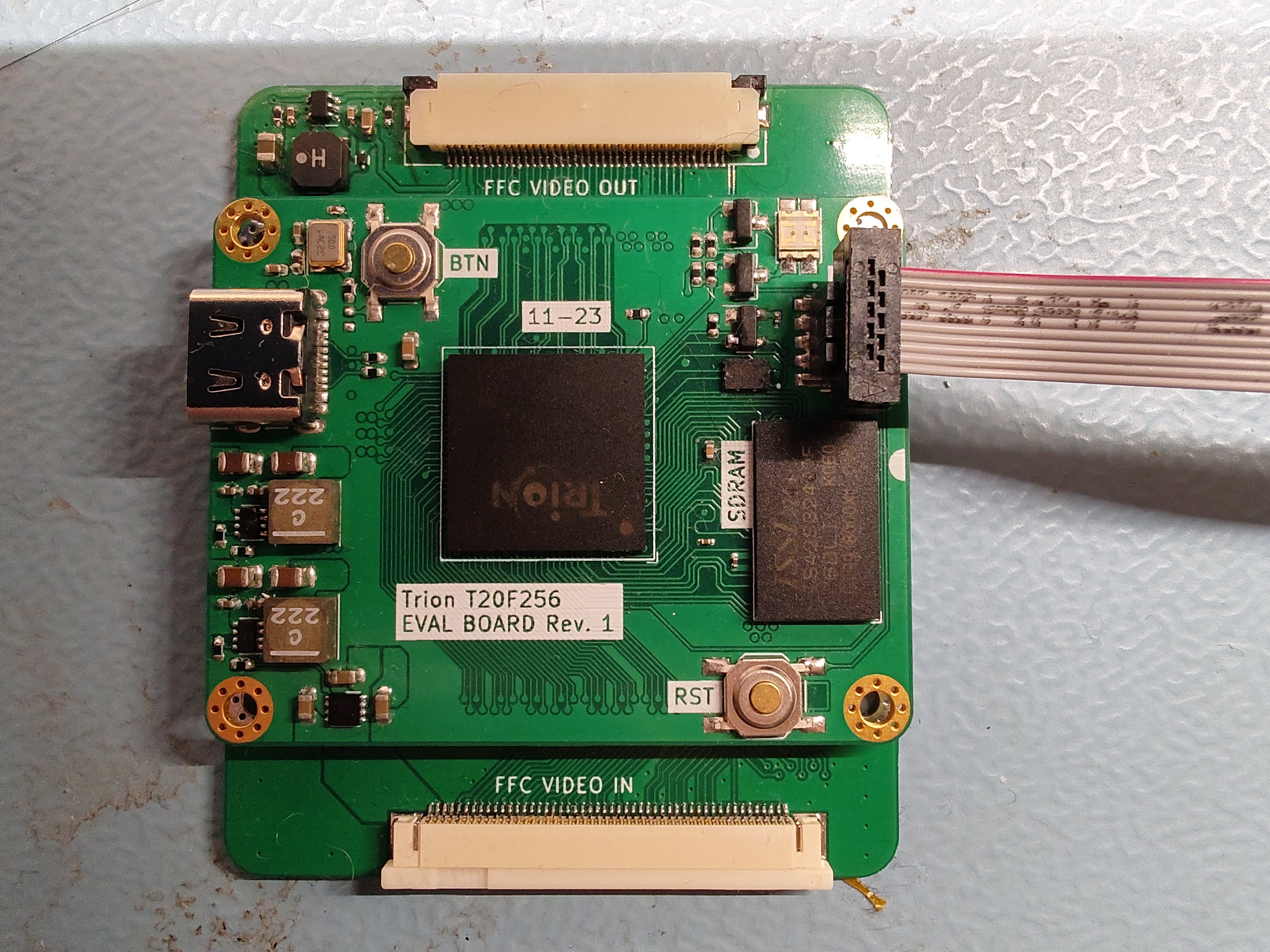
You can imagine the next step…. Custom development board time!
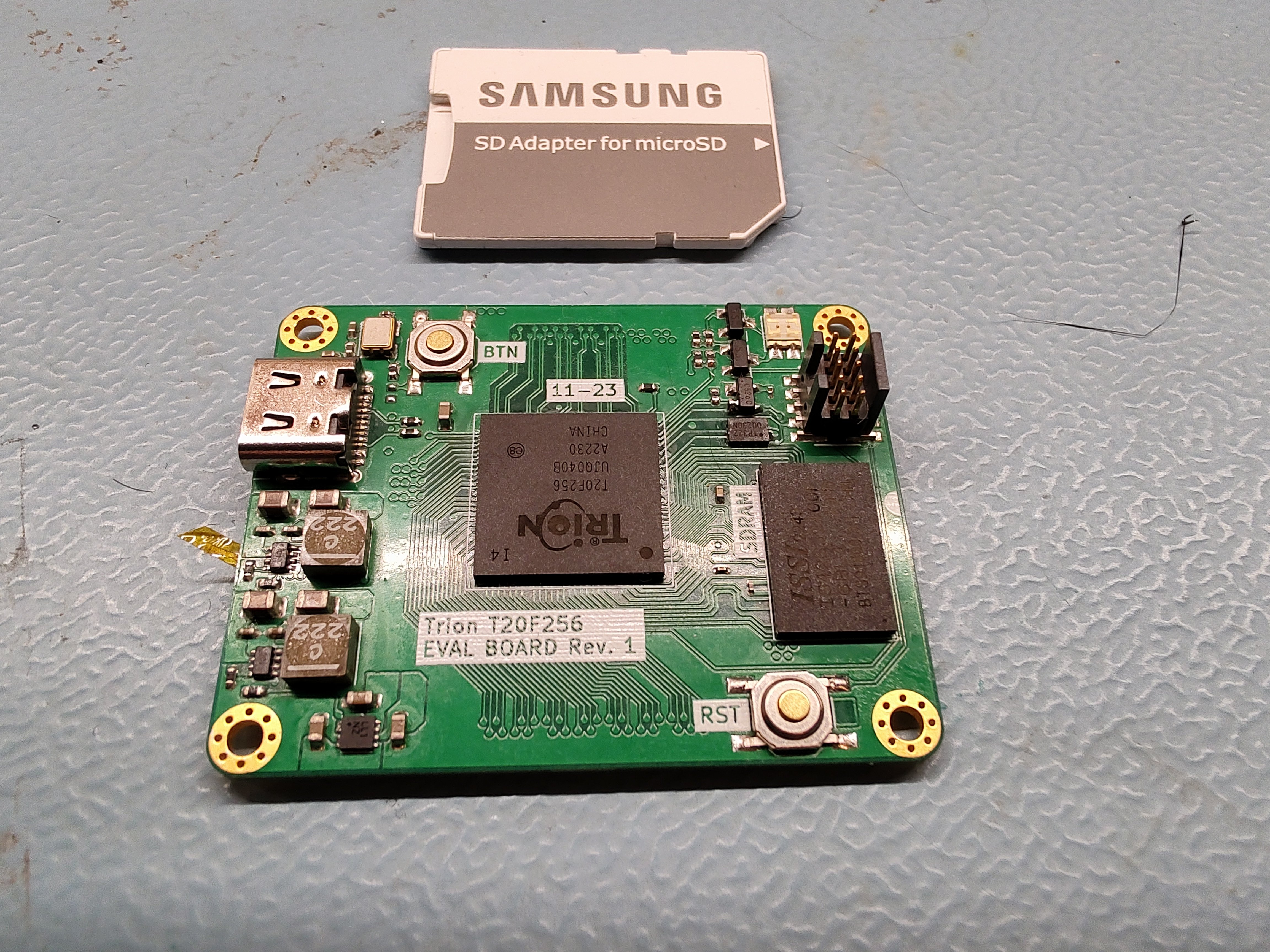
This one was like a 2-weekend project and it should include everything I need to continue with video processing. I tried to check all the boxes regarding compatibility with my existing PS2 mainboard while making it flexible enough to be reusable for future projects. The main features are:
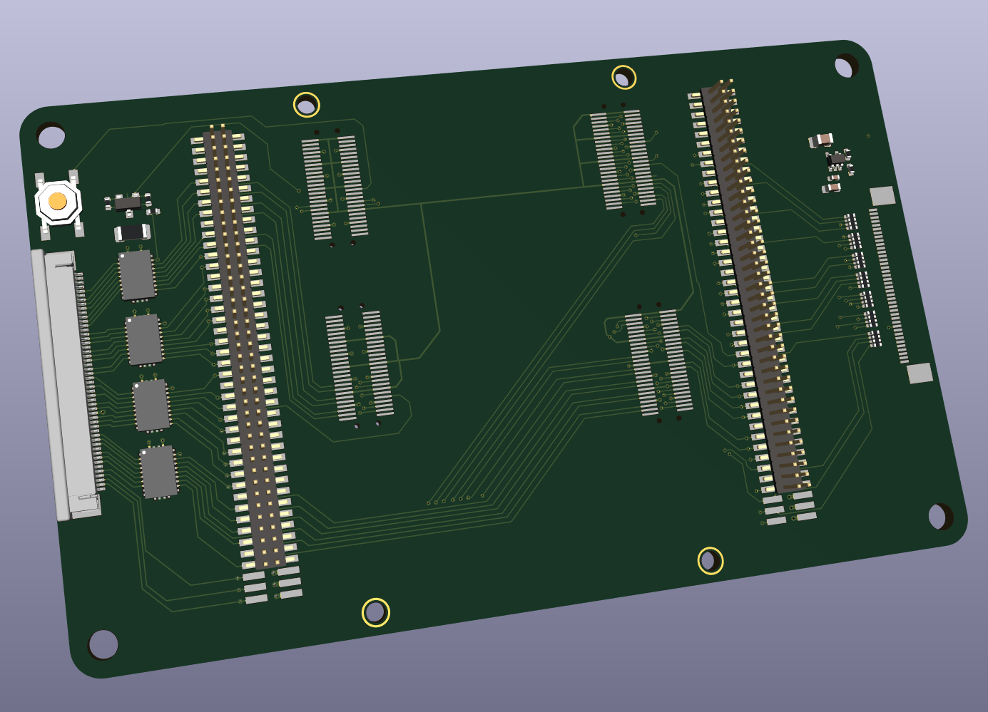
Of course, I also designed a shield for interfacing with my PS2 and the LCD later & a little JTAG programming adapter PCB for the FTDI module:
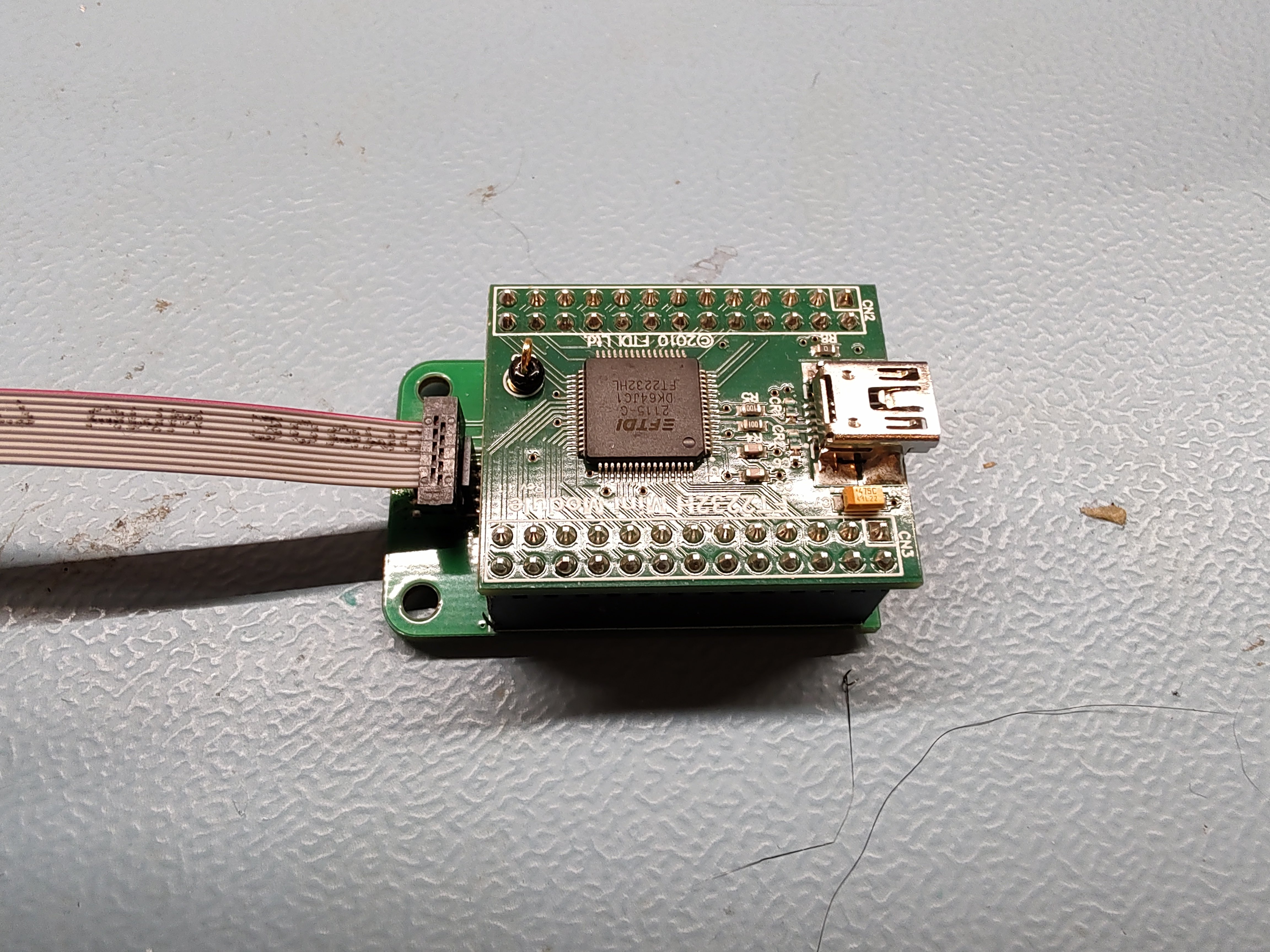
Assembly went smooth, during testing I had to solder three little bodges, though. The main issue was the RST. Short version: Efinix recommends to use a voltage supervisor with manual reset input to drive the reset pin of the FPGA at powerup. The RST signal is also required for JTAG and the application note says to connect all reset inputs to the manual reset input of the voltage supervisor. Doing that will delay all reset pulses from the debugger by ~200ms, which made JTAG programming impossible. I had to connect the JTAG RST to the FPGA directly and solder the voltage supervisor in parallel to handle startup, that fixed it.
With the hardware part done, I can focus on the video interface again. First step is to design a proper framebuffer as the heart of the scaler. That was done in the last 2 weeks over Christmas.
The Efinix SDRAM controller IP did not convince me and making things from scratch is fun, so I decided to design one myself as a learning exercise and to get some experience. I would not call the Efinity IDE and documentation beginner friendly, so it was a good opportunity to experiment with the tools too. There’s not a lot of features compared to vivado; no wizards, no templates, no simulator, no schematic view, no block designs; BUT it’s a million times faster, the entire flow from synthesis to bitstream takes just as long as the synthesis in vivado…I'm still using vivado for functional simulation, though.
Back to the SDRAM: The state machine was straight forward, but it was my first-time debugging timings. In the end I got it working at 150MHz, but at the max of 166MHz the controller just reads garbage still. 166MHz should be achievable according to the timing analysis, but maybe I just have to recalculate my timing constraints to find the culprit.
Anyway 150MHz should be plenty already, in the simulation the controller hits ~400Mbyte/s write and ~300Mbyte/s read MAX when there are no rows to open/close. The video stream should require about 160MByte/s in the worst case.
The controller is optimized for R/W speed over latency and I tried to make it as simple as possible without sacrificing too much of the bandwidth. There are no fancy functions like command scheduling (overlapping, canceling,...) or delaying refresh cycles, only one command at at a time. It does do 8-word read/write bursts, though - to maximize the bandwitdh (that's 32 bytes per command). On top of that it avoids auto-precharges and insteads keeps track of the open rows to minimize overhead. So far the controller is passing all my test cases in simulation (with some generic SDRAM memory model).
My goal is to make the SDRAM controller as stable as possible, as it is one of the core blocks of the scaler & maybe I can still shave off some clock cycles here and there to make it faster.
I will work on that the next week and then I will continue with the other blocks. Missing would be the video input and output blocks (kinda defined already from my experiments), the read/write scheduler for the framebuffer (probably the most complex block), the scaler and the block to write OSD info into the framebuffer. Still a LOT of work ahead!
Sorry, I completely forgot to post updates! (again…)
Ever since the last update I’ve been working on FPGA stuff to get the video output of my mainboard up and running and I guess I’m slowly getting there.
After the little experiments with my DPI LCD I know more or less what to expect when it comes to resolutions and video timings. The big blocker was the lack of memory to buffer at least one field of each frame. It made the bridge between the 2 clocking regions very tricky and at some point it stopped me from progressing with my design.
The next logical step was to look into the available RAM options. First, I wanted to try the DDR3 on my Artix 7 Development board, as it would provide plenty of memory at a sufficient speed.
Getting DDR3 working is not trivial, though. I figured that out the hard way after 2 evenings of fighting with vivado’s memory interface generator IP. That “experience” forced me to take a step back and to reconsider things.
At that point I knew already that I would like to use a cheaper FPGA for the final board and it made no sense to waste time with proprietary Xilinx IP, so instead I was looking into the RAM options with my FPGA of choice, the Trion T20. It didn’t take a lot of reading in the datasheet until I realized that the only package I can economically design a PCB for (0.8mm pitch) does not have a hard DDR3 controller & as I’m by far not experienced enough to write a soft DDR3 controller, that option was out of the game.
Instead, I chose a SDR SDRAM for the framebuffer, the IS42S32400F-6BL to be precise. Compared to DDR3 it mostly has drawbacks: it’s slower, it’s more expensive, SDR RAM is kinda outdated and on top of that it requires more pins. BUT it’s considerably easier to drive and it makes PCB layouting much simpler with less strict timing & impedance requirements.
You can imagine the next step…. Custom development board time!
This one was like a 2-weekend project and it should include everything I need to continue with video processing. I tried to check all the boxes regarding compatibility with my existing PS2 mainboard while making it flexible enough to be reusable for future projects. The main features are:
- Trion T20F256
- IS42S32400F-6BL SDRAM + QSPI flash for the FPGA config
- All power regulators included, only requires 5V to operate
- 2 80 pin mezzanine connectors with as many IOs as I could fit -> great for custom shields
- 1 bank is selectable between 1.8V and 3.3V (mainly for the GS video interface)
- Status LEDs, 1 user button
- Programmable via JTAG (QSPI flash too)
- The BOM of the whole board (including PCB) is less than my old Artix 7 A35 FPGA (just the chip!!)
Of course, I also designed a shield for interfacing with my PS2 and the LCD later & a little JTAG programming adapter PCB for the FTDI module:
Assembly went smooth, during testing I had to solder three little bodges, though. The main issue was the RST. Short version: Efinix recommends to use a voltage supervisor with manual reset input to drive the reset pin of the FPGA at powerup. The RST signal is also required for JTAG and the application note says to connect all reset inputs to the manual reset input of the voltage supervisor. Doing that will delay all reset pulses from the debugger by ~200ms, which made JTAG programming impossible. I had to connect the JTAG RST to the FPGA directly and solder the voltage supervisor in parallel to handle startup, that fixed it.
With the hardware part done, I can focus on the video interface again. First step is to design a proper framebuffer as the heart of the scaler. That was done in the last 2 weeks over Christmas.
The Efinix SDRAM controller IP did not convince me and making things from scratch is fun, so I decided to design one myself as a learning exercise and to get some experience. I would not call the Efinity IDE and documentation beginner friendly, so it was a good opportunity to experiment with the tools too. There’s not a lot of features compared to vivado; no wizards, no templates, no simulator, no schematic view, no block designs; BUT it’s a million times faster, the entire flow from synthesis to bitstream takes just as long as the synthesis in vivado…I'm still using vivado for functional simulation, though.
Back to the SDRAM: The state machine was straight forward, but it was my first-time debugging timings. In the end I got it working at 150MHz, but at the max of 166MHz the controller just reads garbage still. 166MHz should be achievable according to the timing analysis, but maybe I just have to recalculate my timing constraints to find the culprit.
Anyway 150MHz should be plenty already, in the simulation the controller hits ~400Mbyte/s write and ~300Mbyte/s read MAX when there are no rows to open/close. The video stream should require about 160MByte/s in the worst case.
The controller is optimized for R/W speed over latency and I tried to make it as simple as possible without sacrificing too much of the bandwidth. There are no fancy functions like command scheduling (overlapping, canceling,...) or delaying refresh cycles, only one command at at a time. It does do 8-word read/write bursts, though - to maximize the bandwitdh (that's 32 bytes per command). On top of that it avoids auto-precharges and insteads keeps track of the open rows to minimize overhead. So far the controller is passing all my test cases in simulation (with some generic SDRAM memory model).
My goal is to make the SDRAM controller as stable as possible, as it is one of the core blocks of the scaler & maybe I can still shave off some clock cycles here and there to make it faster.
I will work on that the next week and then I will continue with the other blocks. Missing would be the video input and output blocks (kinda defined already from my experiments), the read/write scheduler for the framebuffer (probably the most complex block), the scaler and the block to write OSD info into the framebuffer. Still a LOT of work ahead!