mokus
.
- Joined
- Apr 12, 2020
- Messages
- 23
- Likes
- 76
I've started work this weekend on a design for a flexible PCB (actually two most likely) intended to act as an electrical interface between a trimmed Wii and the rest of a portable or mini build. Adhering to the ways of the ancients, I have given it a stupid punny name with two i's. By basing it on a recent meme, I have also guaranteed the name will age as badly as possible, for ultimate cringe.
Anyway, all that aside, some details. The project is hosted at https://github.com/mokus0/WiirdFlex, and is designed in Altium (I normally use KiCad for my open stuff, but this one is a lot more mechanically intricate and I can do it much faster in Altium).
This is my first worklog on BitBuilt, so bear with me while I figure out how to post images, the best way to organize it, etc.
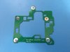
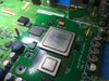
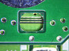
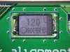
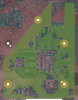
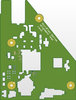
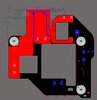
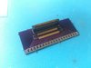
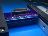
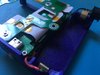
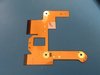
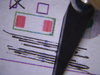
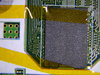
As an introduction, here's my first fit and alignment check, and an alignment check test fixture I just ordered:
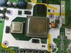
It fits quite well, perfect up to the limits of my crappy inkjet printer's accuracy and my own skill with an X-Acto.
What I've done so far:
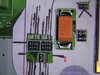
I started on Friday by digging through the RVK-01 Compendium, surveying it to develop a general plan (what signals I need, where to get them, etc). Next was to measure the size and location of the mounting holes, main ICs and their bulk capacitors, using a combination of calipers and cross-checking with the Compendium. From those measurements I created footprints for the mounting holes and capacitors, and keep-outs for the ICs and the impedance controlled areas around them (I'll use that space if I need to, but prefer not to). I also added another pad for the 3x3 array of vias on the 1.8v net. At this stage, the goal is to get accurate measurements of where everything is on the Wii, not necessarily to put the design down for actually making those connections.
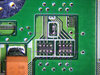
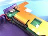
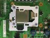
At this point, it looked like this awful photo of my screen:
Arbitrarily, I selected an origin: the bottom left mounting hole (in Compendium orientation). All footprints are using this point as their origin, so once the footprints themselves incorporate proper alignment, the PCB layout for these parts is as simple as setting them all to the same X/Y coordinates.
On Saturday (yesterday), I continued with some more measurements, more footprints for more stuff, etc. Along the way, my copy of the compendium gained a lot of extra layers including a bunch of measurement reference marks and a copy of someone's trim outline graphic (edited to just the cut lines so it can overlay everything). It seems the copper layers are quite well scaled and rectified, so over time I gained the confidence to spend less time measuring the Wii itself and relied more on the GIMP measuring tools, just spot-checking here and there.
Eventually I got to the point where I needed to fine-tune things more aggressively, so I set up an output job from Altium to produce a 1:1 scale PDF of the design. From that, it's a little tedious but I can export from altium, import as a layer to GIMP (600 dpi to match the Compendium), select all white pixels and delete, drag-select a rectangle around the board image, crop the layer, then move the layer into place (using the mounting holes as a visual alignment reference).
After a few dozen iterations of that, tweaking part placement and board edges along the way, I printed the board out, sat down with an X-acto and a microscope, and produced a paper Wii Gasket that looked like the one I posted above. From a distance, anyway. I discovered that "measure twice, cut once" does not extend to all even numbers - in particular, it doesn't scale down to "measure zero times, cut once".
What is this, a WiiFlex for ants?
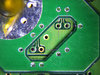
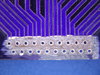
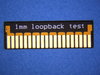
After re-checking that, yes, my Altium output really was 1:1, I decided to print again using a different program. Apparently FireFox's built-in PDF viewer doesn't care too much about printing things at the size indicated in the document. Back to GIMP, back to the microscope, and back to work. Finally, the payoff:
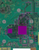
This is the same image as at the top again. I had to manually widen the holes for the capacitors and add a couple more cutouts by eye (the areas around U5 and C4), which I then incorporated into the Altium design.
The black pen marks you can see in the image might be worth explaining a bit too. Using the X-acto blade as a straightedge, I added those marks to create crosshairs centered on each of the target pads and vias. Then I cut out the area around those vias, leaving the outer parts of the crosshairs. Finally, after placing the board down I then used the X-acto again to check that the lines crossed the things they were supposed to cross. For example:
At this point, I now have pretty great confidence in the workflow, which is good because the bottom is going to be a lot trickier. To everyone who worked on the Compendium: THANK YOU ALL SO MUCH, it has been a fantastic reference.
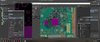
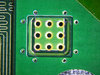
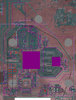
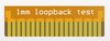
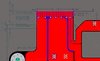
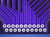
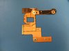
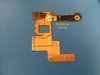
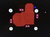
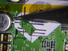
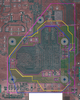
The next step was to take the design and convert it to something I could test-fit more accurately. My printer is crap, my pen has a fine tip but is still pretty big compared to the accuracy I'm trying to measure, and paper is flexible and even stretchy when cut up so much, so although this method of measurement gives me _some_ confidence, I want more. So I took the crosshair concept and applied it to alternate versions of the footprints on the board. This involved creating cut-outs around the target pads and vias, and small drilled holes all around them. These holes are aligned so that thin wire drawn through them should cross at exactly the point where I believe the target pad _should_ be. Here's a close-up of the concept (the thin pink lines show where the wire would go):
For larger pads like the capacitors, the wire should end up outlining the pad. For smaller ones like the SD pads and USB vias, the wire should end up crossing at exactly where I want the flex board to attach. For the bluetooth traces, the wires should end up aligned exactly to the traces.
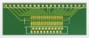
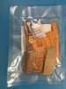
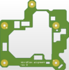
And finally, that brings us up to date. This morning I looked around at board houses, picked one (Seeed Fusion for this board), made some small adjustments to meet the board house's design rules, and ordered ten of these (again, same photo as top):
Next I'll probably start work on the bottom side initial layout, and hopefully when I do get the top side alignment board back there aren't too many surprises. And hopefully the order doesn't get delayed too badly due to COVID-19.
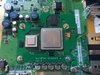
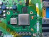
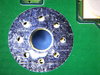
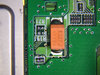
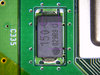
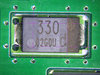
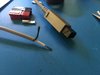
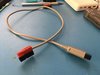
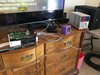
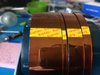
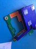
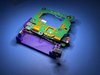
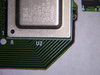
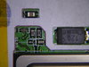
I think that's all for now. Here are a few more random photos:
Anyway, all that aside, some details. The project is hosted at https://github.com/mokus0/WiirdFlex, and is designed in Altium (I normally use KiCad for my open stuff, but this one is a lot more mechanically intricate and I can do it much faster in Altium).
This is my first worklog on BitBuilt, so bear with me while I figure out how to post images, the best way to organize it, etc.
As an introduction, here's my first fit and alignment check, and an alignment check test fixture I just ordered:
It fits quite well, perfect up to the limits of my crappy inkjet printer's accuracy and my own skill with an X-Acto.
What I've done so far:
I started on Friday by digging through the RVK-01 Compendium, surveying it to develop a general plan (what signals I need, where to get them, etc). Next was to measure the size and location of the mounting holes, main ICs and their bulk capacitors, using a combination of calipers and cross-checking with the Compendium. From those measurements I created footprints for the mounting holes and capacitors, and keep-outs for the ICs and the impedance controlled areas around them (I'll use that space if I need to, but prefer not to). I also added another pad for the 3x3 array of vias on the 1.8v net. At this stage, the goal is to get accurate measurements of where everything is on the Wii, not necessarily to put the design down for actually making those connections.
At this point, it looked like this awful photo of my screen:
Arbitrarily, I selected an origin: the bottom left mounting hole (in Compendium orientation). All footprints are using this point as their origin, so once the footprints themselves incorporate proper alignment, the PCB layout for these parts is as simple as setting them all to the same X/Y coordinates.
On Saturday (yesterday), I continued with some more measurements, more footprints for more stuff, etc. Along the way, my copy of the compendium gained a lot of extra layers including a bunch of measurement reference marks and a copy of someone's trim outline graphic (edited to just the cut lines so it can overlay everything). It seems the copper layers are quite well scaled and rectified, so over time I gained the confidence to spend less time measuring the Wii itself and relied more on the GIMP measuring tools, just spot-checking here and there.
Eventually I got to the point where I needed to fine-tune things more aggressively, so I set up an output job from Altium to produce a 1:1 scale PDF of the design. From that, it's a little tedious but I can export from altium, import as a layer to GIMP (600 dpi to match the Compendium), select all white pixels and delete, drag-select a rectangle around the board image, crop the layer, then move the layer into place (using the mounting holes as a visual alignment reference).
After a few dozen iterations of that, tweaking part placement and board edges along the way, I printed the board out, sat down with an X-acto and a microscope, and produced a paper Wii Gasket that looked like the one I posted above. From a distance, anyway. I discovered that "measure twice, cut once" does not extend to all even numbers - in particular, it doesn't scale down to "measure zero times, cut once".
What is this, a WiiFlex for ants?
After re-checking that, yes, my Altium output really was 1:1, I decided to print again using a different program. Apparently FireFox's built-in PDF viewer doesn't care too much about printing things at the size indicated in the document. Back to GIMP, back to the microscope, and back to work. Finally, the payoff:
This is the same image as at the top again. I had to manually widen the holes for the capacitors and add a couple more cutouts by eye (the areas around U5 and C4), which I then incorporated into the Altium design.
The black pen marks you can see in the image might be worth explaining a bit too. Using the X-acto blade as a straightedge, I added those marks to create crosshairs centered on each of the target pads and vias. Then I cut out the area around those vias, leaving the outer parts of the crosshairs. Finally, after placing the board down I then used the X-acto again to check that the lines crossed the things they were supposed to cross. For example:
At this point, I now have pretty great confidence in the workflow, which is good because the bottom is going to be a lot trickier. To everyone who worked on the Compendium: THANK YOU ALL SO MUCH, it has been a fantastic reference.
The next step was to take the design and convert it to something I could test-fit more accurately. My printer is crap, my pen has a fine tip but is still pretty big compared to the accuracy I'm trying to measure, and paper is flexible and even stretchy when cut up so much, so although this method of measurement gives me _some_ confidence, I want more. So I took the crosshair concept and applied it to alternate versions of the footprints on the board. This involved creating cut-outs around the target pads and vias, and small drilled holes all around them. These holes are aligned so that thin wire drawn through them should cross at exactly the point where I believe the target pad _should_ be. Here's a close-up of the concept (the thin pink lines show where the wire would go):
For larger pads like the capacitors, the wire should end up outlining the pad. For smaller ones like the SD pads and USB vias, the wire should end up crossing at exactly where I want the flex board to attach. For the bluetooth traces, the wires should end up aligned exactly to the traces.
And finally, that brings us up to date. This morning I looked around at board houses, picked one (Seeed Fusion for this board), made some small adjustments to meet the board house's design rules, and ordered ten of these (again, same photo as top):
Next I'll probably start work on the bottom side initial layout, and hopefully when I do get the top side alignment board back there aren't too many surprises. And hopefully the order doesn't get delayed too badly due to COVID-19.
I think that's all for now. Here are a few more random photos:
Last edited: